Ensemble RXTX - TX Mixer (QSE)
Band: 30, 20, 17m
Introduction
Band Specific Components
This stage involves band-specific components and is currently configured for the 30, 20, 17m band. If you need to configure this page for a different band, click on the "Band" tab in the menu above. This would take you to the home page, where you can select the new band and then return to this page.
General Info About the Stage
You may want to follow along with George, W5JDX, in his HamNation podcast #80, in which he completes the TX Mixer and TX Driver/PA stages. The clip begins at minute 47 in the podcast.
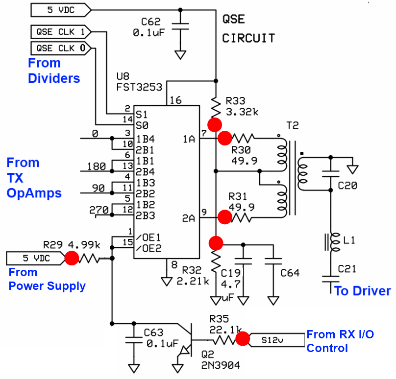
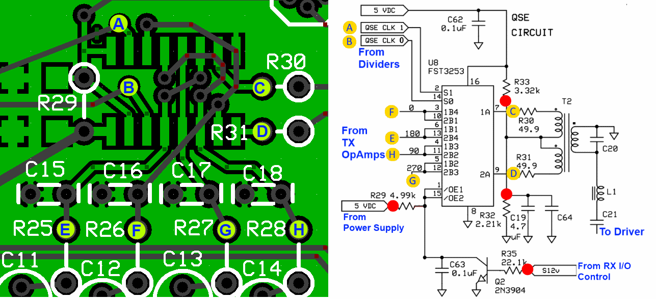
This stage adds the TX Mixer to the board and provides the modulation of the Dividers' output signals by the 4 I and Q signals from the TX OpAmps (Quadrature Sampling Exciter - QSE). The result is a double sideband RF waveform that will be coupled into the PA Stage.
Theory of Operation
Let's suppose you were working 40m with a SDR center frequency of 7.056 MHz. You have tuned your SDR (via the software) so that you are listening to a CW station on 7.066 MHz (10 kHz up from the center frequency).
If you were to listen to the I and Q signals from the hardware RX via an amplifier or headphones (assuming there were no other signals and little noise) you would hear a single 10 kHz CW signal on both channels. Your ears may or may not be able to detect the fact that the tone in one ear is 90 degrees out of phase (I.e., In quadrature) with the tone in the other ear.
By comparing the phase change between the I/Q signals the SDR RX software determines that this signal is 10KHz higher than the center frequency and displays the CW signal as a broken line on the waterfall. It also frequency shifts this signal at the output of the soundcard so it is heard at as normal CW tone from the speakers.
Now, assume you decide to transmit on that frequency where you have placed your cursor (7.066 MHz). Your SDR software will emit a 10 kHz signal (the delta between the center frequency and the selected TX frequency) in both the I and Q outputs. The I and Q outputs will differ in phase by one-fourth of a cycle of the 10kHz signal, or 90 degrees. These signals will go into the SDR hardware on the TX side, through the TX OpAmps and into the TX Mixer, where it will beat up against the LO center frequency of 7.056 MHz.
The input to the mixer consists of four 10KHz signals from the TX OpAmps and two quadratures LO signals; the output from the mixer is the RF product of the LO and the input 10 kHz signal. If you were to listen to the input 10 kHz signal you would hear a tone. This tone is audible simply because it represents the delta between the center frequency and the desired transmit frequency, in this case, only 10 kHz, and, since it is in the range of audio frequencies, is audible. If you were to select a higher frequency on whch to transmit, say 7.080 MHz, the resultant signal would be a 24 kHz signal; perhaps your dog would hear it, but you certainly would not! However, the TX Mixer will happily upconvert this to an RF product!
The TX OpAmps are unity gain inverting (180 degrees phase change) amplifiers. The I and Q signals are each inverted by a unity gain amplifier, followed by a second inversion of each signal. (Note, two successive 180 degree changes, gets us back to 0 degrees.) Outputs are taken from each of the four amplifiers, resulting in I outputs of 0 and 180 degrees, and Q outputs of 90, and 270 degree phase. Each of the four are then input to the TX Mixer and are switched ("mixed") by the LO signals which are also 90 degrees apart in phase). The two outputs of the mixer are the up-converted RF products, in anti-phase (I.e., 180 degrees apart). The FST3253 mixer switches each of the 4 I/Q signals to each of the two primary windings of T2 at specific time intervals. The signals on these two windings are the outputs of the mixer and are the up-converted RF products. When these RF products are combined in the input transformer (T2) of the Driver/PA Stage. an undesired "image" signal will be cancelled out, leaving a single SSB signal to be amplified by the PA. In this example, the desired SSB signal would be at 7.066 MHz and the image signal would be at 7.046MHz, if not cancelled out. Errors in the phase or amplitude of any of the four I/Q signals going into the mixer stage will result in less than desired unwanted sideband suppression. If there is unbalance in the signals going into the two primary windings of T2, or unbalance in the two windings due to poor solder connections (or possibly shorted turns in one of the windings) then the image signal will likely appear. The software will adjust the phase and level of the I/Q signals such that the suppression of the undesired sideband can be maximized. However, suppression of the image signal is dependent on close matching of the circuit components around T2 and the matching of the two primaries of T2. With careful adjustment of the SDR software one can obtain good sideband suppression and an image free output from the TX Mixer's T2.
In summary, the SDR software sends two suitably phased audio (or ultrasonic) signals from the soundcard that are up-converted (i.e. shifted to RF frequencies) by the TX mixer, amplified, and filtered in the PAF board.
Note: the above description relates to the traditional "Softrock/Rocky/Winrad/Genesis fixed center frequency" paradigm. In the PowerSDR paradigm, things are a little different. On receive, all versions of PSDR (other than the Genesis version) make use of a pseudo IF system, nominally set at 9kHz. When you go to transmit, the LO frequency is shifted by 9kHz so that it is actually at the wanted TX frequency. That has the distinct advantage that the TX image rejection is always carried out a the same sound card frequency range, i.e. DC to say 3 or 4kHz.
For Rocky and the Genesis PSDR version, both use a 'fixed' LO for their centre frequency, so when you transmit, the sound card has to generate an output at whatever frequency offset you are 'tuned' to, so if you were 30kHz below the centre frequency, then the soundcard I/Q output would be 30kHz and the TX 'audio' signal. Doing it that way means the TX image rejection is always compromised as it cannot be optimised at a single point, as you could be transmitting anywhere +/- the sound card sampling rate.
Summary Build Notes
Stage Schematic
Go to Top of Page
Click here for full schematic
(Red dots represent the "hairpin" (or left-hand or topmost) lead of the component)
Board Layouts
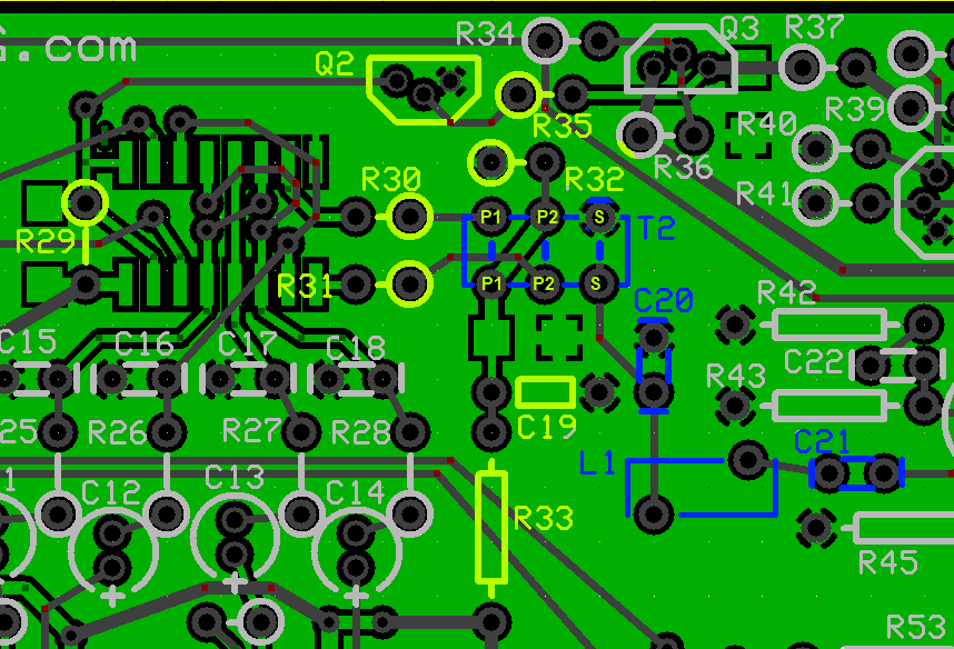
Board Top
Go to Top of Page
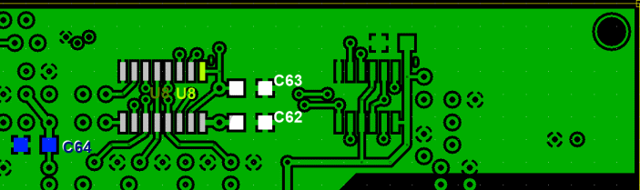
Board Bottom
Go to Top of Page
TX Mixer (QSE) Bill of Materials
(30, 20, 17m band option)
(details for installation of each component are provided in the step instructions, further down the page)
Be sure to use the correct wire gauge when winding inductor(s)
| Check | Type | Category | Component | Count | Marking | Image |
|---|---|---|---|---|---|---|
| ☐ | Capacitor | Ceramic | 82 pF | 2 | 82J |

|
| ☐ | Capacitor | SMT 1206 | 0.1 uF | 3 | (smt) black stripe |

|
| ☐ | Capacitor | Ceramic | 4.7 uF 10% 16V X7R RAD | 1 | 475 |
|
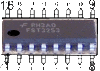
| ☐ | IC | SOIC-16 | FST3253 mux/demux switch | 1 | FST3253 ESD!!! |
|
| ☐ | inductor | Toroid | T30-6 toroid core | 2 | yellow |

|
| ☐ | Inductor | Coil | 1.6uH 21T #30 on T30-6 (yellow) | 1 | yellow | (magnetic wire) |
| ☐ | Inductor | Xfrmr | 1.74uH 11T bifilar/22T #30 on T30-6(yellow) | 1 | yellow | (magnetic wire) |
| ☐ | Resistor | 1/4W | 49.9 ohm 1% | 2 | yel-wht-wht-gld-brn |

|
| ☐ | Resistor | 1/4W | 2.21 k 1/4W 1% | 1 | r-r-br-br-br |

|
| ☐ | Resistor | 1/4W | 3.32 k 1/4W 1% | 1 | ora-ora-red-brn-brn |

|
| ☐ | Resistor | 1/4W | 4.99 k 1/4W 1% | 1 | y-w-w-br-br |

|
| ☐ | Resistor | 1/4W | 22.1 k 1/4W 1% | 1 | r-r-brn-r-br |

|
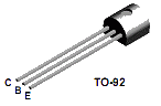
| ☐ | Transistor | TO-92 | 2N3904 NPN Transistor | 1 | 2N3904 |
|
Go to Top of Page
Detailed Build Steps
Step_Wind and Install Inductors
Inductor Information
Common Techniques:
- Wire Gauge: remember the higher the number, the thinner the wire. E.g., #30 wire is thinner than #26 wire.
-
One turn:
- For toroids, one turn is a single pass through the center hole.
- For binocular cores, one turn is a pass in which the wire goes in the bottom, comes out the top, goes back in the other hole at the top, and comes out the other hole at the bottom.
- Bi (tri) filar means 2(3) equal lengths of wire. You get the bi(tri)filar strand by taking the length of wire specified for the primary winding, folding it into half(thirds), twisting it to 3~ twists per inch, and winding it over the primary winding. One end of such a strand will have two(three) leads; the other end will have a "hairpin" bend (and a single lead in the case of tri-filar).
- Multi-filar windings are usually done AFTER the uni-filar winding is done.
- Windings shoud be evenly spaced and ideally made such that the winding covers ~345 degrees of the toroid
- Inductance values given are for the single (uni-filar) winding. They are provided to help verify turn counts and core material selected. It's often reported inductances are higher using the theoretical number of turns as calculated by the manufacturer's windings calculator tool, e.g. http://toroids.info/. Normally though these are not too critical, especially with the LF bands antenna noise will still be seen.
-
Toroid nomenclature provides the outside diameter of the toroid (in hundredths
of an inch - the "30" in "T30-2"), and material code (the "2" in "T30-2").
Color codes used in these kits are:
- 2=Red
- 3=Gray
- 6=Yellow
- 7=White
- 10=Black
- 12=Green (with White on opposite side)
Inductors In This Step
L1COIL: 1.6uH 21T #30 on T30-6 (yellow)
Using approximately 14 inches of #30 wire, wind 21 turns on a 0.30 inch od T30-6 (yellow) ferrite. Inductance = 1.60 uH.
XFRMR: 1.74uH 11T bifilar/22T #30 on T30-6(yellow)
Primary: Using approximately 14 inches of #30 wire, wind 11 turns , bifilar, on a 0.30 inch od T30-6 (yellow) ferrite.
Secondary: Using 14 inches of #30 wire, wind 22 turns on the ferrite in the same direction as the primary winding. Inductance of the single winding (usually the primary) is 1.74 uH.
See WB5RVZ Inductor Construction Hints for hints on winding and installing inductors.
You want to wind and install and then continuity-test these inductors BEFORE installing the other components to the topside of the board.
Inductor Continuity Tests
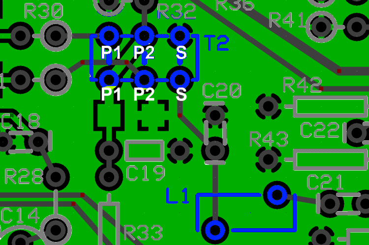
After installiing T2 and L1, you can test their soldering and continuity using your ohmmeter and the test points indicated below: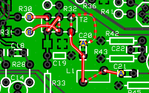
| Check | Designation | Component (top/bottom) | Orientation | Marking | Image | Band | Notes |
|---|---|---|---|---|---|---|---|
| ☐ | L1 | 1.6uH 21T #30 on T30-6 (yellow) (top) | yellow |
 |
30, 20, 17m | ||
| ☐ | L1-core | T30-6 toroid core (top) | yellow |
|
30, 20, 17m | ||
| ☐ | T2 | 1.74uH 11T bifilar/22T #30 on T30-6(yellow) (top) | yellow |
|
30, 20, 17m | 2x8" / 14" | |
| ☐ | T2-core | T30-6 toroid core (top) | yellow |
|
30, 20, 17m |
Go to Top of Page
Step_Install Topside Components
Be careful and do not get the 2N3904 transistor (Q2) mixed up with the 2N3906 transistor (Q3).
| Check | Designation | Component (top/bottom) | Orientation | Marking | Image | Band | Notes |
|---|---|---|---|---|---|---|---|
| ☐ | C19 | 4.7 uF 10% 16V X7R RAD (top) | 475 |
|
any | ||
| ☐ | C20 | 82 pF (top) | 82J |
|
30, 20, 17m | ||
| ☐ | C21 | 82 pF (top) | 82J |
|
30, 20, 17m | ||
| ☐ | Q02 | 2N3904 NPN Transistor (top) | 2N3904 |
|
any | ||
| ☐ | R29 | 4.99 k 1/4W 1% (top) | N-S | y-w-w-br-br |
|
any | |
| ☐ | R30 | 49.9 ohm 1% (top) | E-W | yel-wht-wht-gld-brn |
|
any | |
| ☐ | R31 | 49.9 ohm 1% (top) | E-W | yel-wht-wht-gld-brn |
|
any | |
| ☐ | R32 | 2.21 k 1/4W 1% (top) | W-E | r-r-br-br-br |
|
any | |
| ☐ | R33 | 3.32 k 1/4W 1% (top) | flat-vert | ora-ora-red-brn-brn |
|
any | |
| ☐ | R35 | 22.1 k 1/4W 1% (top) | W-E | r-r-brn-r-br |
|
any |
Go to Top of Page
Step_Install Bottomside Components
| Check | Designation | Component (top/bottom) | Orientation | Marking | Image | Band | Notes |
|---|---|---|---|---|---|---|---|
| ☐ | C62 | 0.1 uF ((bottom)) | (smt) black stripe |
|
any | ||
| ☐ | C63 | 0.1 uF ((bottom)) | (smt) black stripe |
|
any | ||
| ☐ | C64 | 0.1 uF ((bottom)) | (smt) black stripe |
|
30, 20, 17m | ||
| ☐ | U08 | FST3253 mux/demux switch ((bottom)) | FST3253 ESD!!! |
|
any |
Take extreme care working with this component. Always use ESD precautions.
|
Go to Top of Page
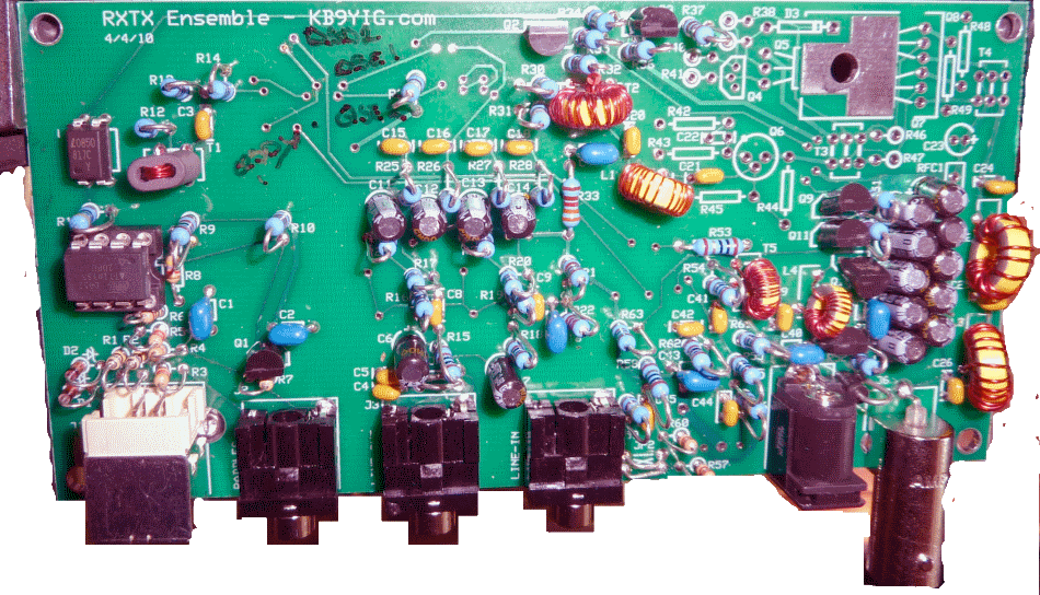
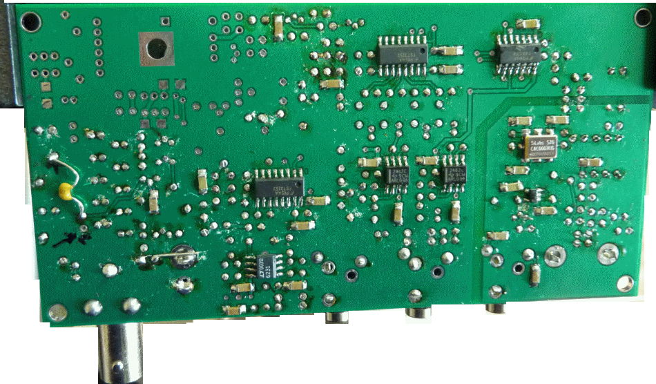
Completed Photos
View of Completed Topside
View of Completed Underside
Go to Top of Page
Progressive Schematic
Where are we in our progress towards the finish line? Click here to view the entire schematic with the completed stages shaded in a yellowish tinge and the remaining stages tinted in blue (the current stage is untinted).
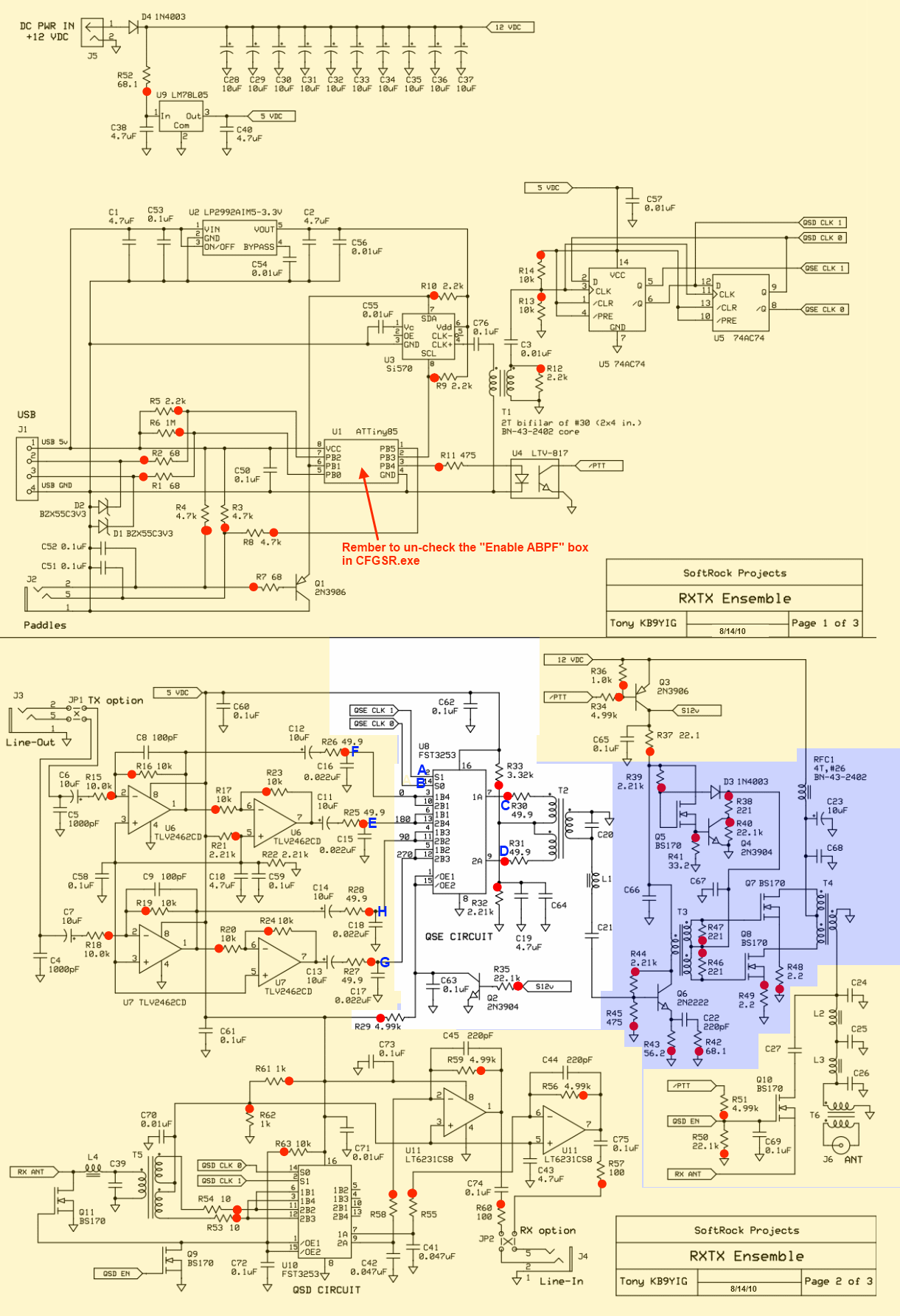
Test the TX Mixer (QSE) Stage
TX Mixer (QSE) - Current Draw
Measure the current draw of the board with 12V power and with 12V power AND USB Power
Go to Top of Page
Test Steps (if any)
| Step | Test Point | UOM | Nominal | Author's | Builder's |
|---|---|---|---|---|---|
| 0 | Current draw with 12V Power only | mA | < 35 | 27.5 | |
| 1 | Current draw with 12V Power AND USB power | mA | < 33 | 25.1 |
Go to Top of Page
TX Mixer (QSE) - Pin Voltages
Activate PTT. (As an alternative to using the SDR Software to activate PTT, you can use a cliplead to ground the top left-hand lead of U4, activating PTT.)
Connect USB and apply power
Measure the voltages at the noted pins (and their pads) for the FST 3253 (U8)
The voltage tests for pins 2 and 4 show a nominal expected value of 2.5 V. Many digital meters do not cope well with the square wave that is present here.On tests where this square wave is present the values to cause concern are those close to 0V or 5V, that shows there is no square wave (thanks to Alan G4ZFQ).
If the voltages are off:
It is likely that U8 is either not being enabled (enable is 0 volts on pins 1 and 15 when PTT is activated) or not being clocked by the square wave QSE signals on pins 2 and 14. The voltage value for measurements C through H is set by the voltage divider of R33/R32. You should double check the values of these resistors. When U8 is enabled and clocked by the QSE this divided voltage is reflected back through the chip for measurements E-H.
Check to see that pins 1/15 are going low when PTT is activated. If not then check the hairpin of R35. It should go high when PTT is on.
(Thanks to Warren Allgyer, K8TOD, for this hint.
Go to Top of Page
Test Steps (if any)
| Step | Test Point | UOM | Nominal | Author's | Builder's |
|---|---|---|---|---|---|
| 0 | A: Pin 2 | Vdc | 2.5 | 2.47 | |
| 1 | B: Pin 14 | Vdc | 2.5 | 2.47 | |
| 2 | C: Pin 7 (R30 hairpin) | Vdc | 2 | 1.99 | |
| 3 | D: Pin 9 (R31 hairpin) | Vdc | 2 | 1.99 | |
| 4 | E: Pin 13 (R25 hairpin) | Vdc | 2 | 1.99 | |
| 5 | F: Pin 10 (R26 hairpin) | Vdc | 2 | 1.99 | |
| 6 | G: Pin 12 (R27 hairpin) | Vdc | 2 | 1.99 | |
| 7 | H: Pin 11 (R28 hairpin) | Vdc | 2 | 1.99 |
Go to Top of Page