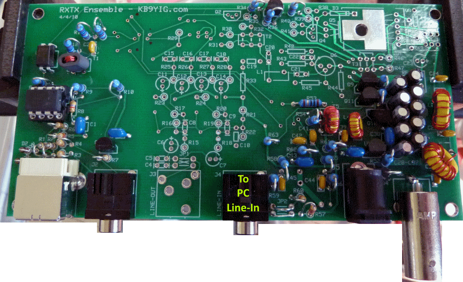
Ensemble RXTX - RX Opamps and Output
Band: 30, 20, 17m
Introduction
General Info About the Stage
You can see the continuing saga of George W5JDX's Solder Smoke project to build this kit. He finishes this stage at minutes 50:10 of HamNation Episode#77.
This stage accepts, as input, the down-converted "chunk" of spectrum containing the signals occurring either side of the center frequency set by the Quadrature Clock Generator (Dividers). This "chunk" is in the base-band, at frequencies ranging from zero to (roughly) 100 kHz or so. There are "I" (In-Phase) and a "Q" (Quadrature) signals, each identical in all respects except phase (90 degrees difference).
The "I" and "Q" signals are amplified in this high-gain op-amp and output to the "Line-In" jack for input to the PC's soundcard's "Line-In" jack. A very important aspect of this latter is that the PC's soundcard MUST be capable of accepting STEREO inputs. If the input to the soundcard is MONO, the radio will not work correctly, and you will see identical, "mirror" images on either side of the center frequency in the spectrum display of the SDR program..
At the completion of this stage, you should have and be able to exercise RX capability!.
Theory of Operation
Warren Allgyer, 9V1TD, has written an excellent posting on the Softrock40 reflector titled "Benchmarking the RX". There is some excellent theoretical and practical information, including suggestions for determining whether your RX is putting out adequate signal strength.
Summary Build Notes
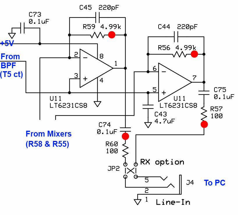
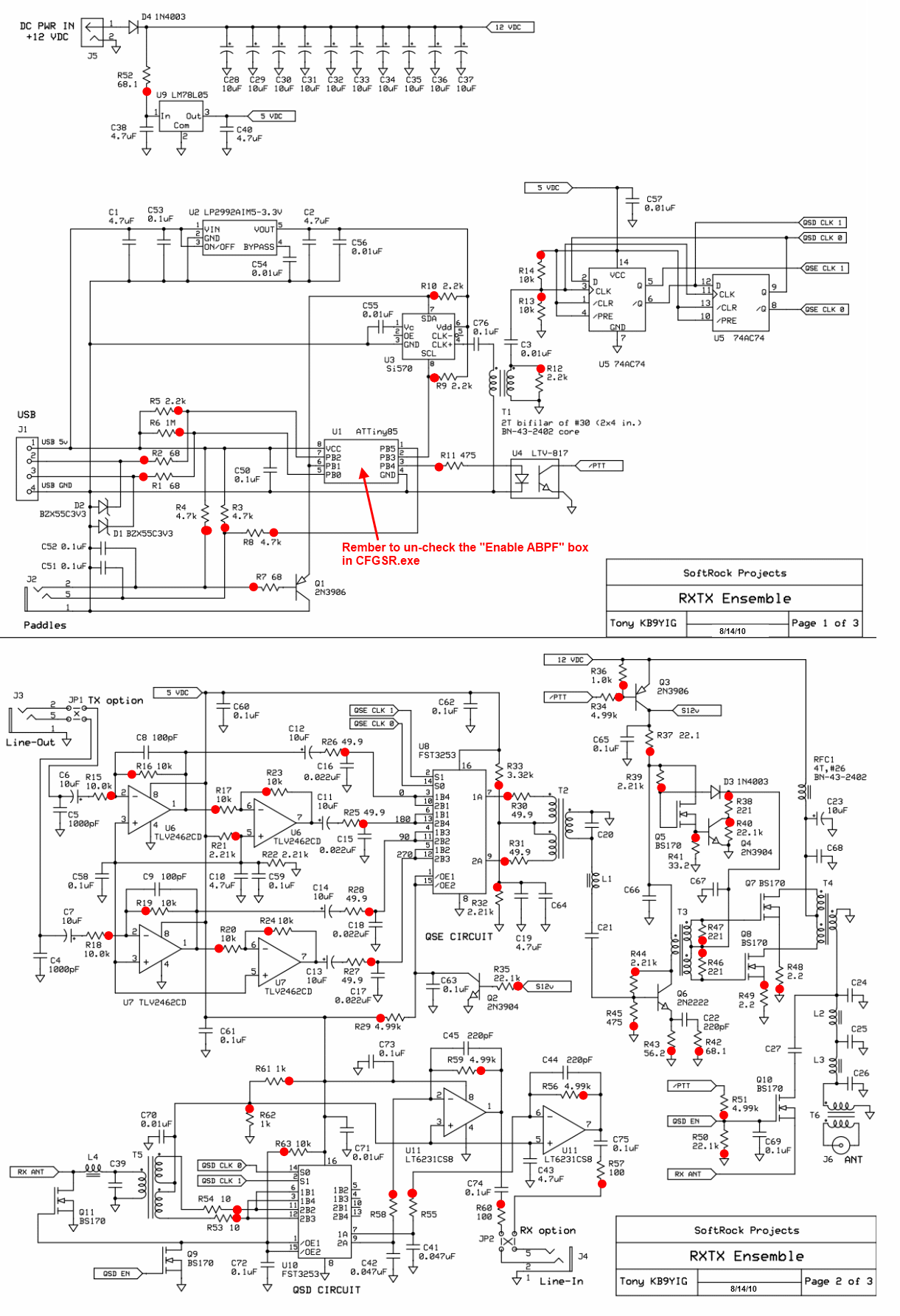
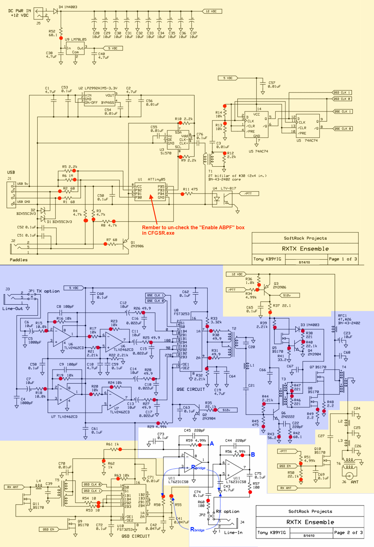
Stage Schematic
Go to Top of Page
Click here for full schematic
(Red dots represent the "hairpin" (or left-hand or topmost) lead of the component)
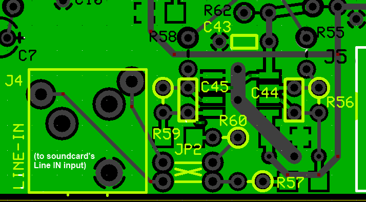
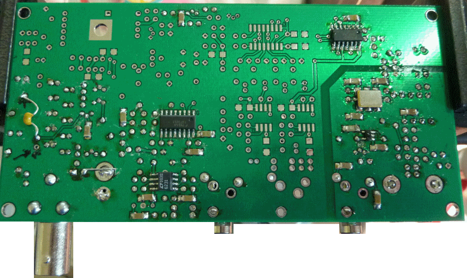
Board Layouts
RX Opamps and Output Bill of Materials
(30, 20, 17m band option)
(details for installation of each component are provided in the step instructions, further down the page)
| Check | Type | Category | Component | Count | Marking | Image |
|---|---|---|---|---|---|---|
| ☐ | Capacitor | Ceramic | 220 pF 5% | 2 | 221 |
|
| ☐ | Capacitor | SMT 1206 | 0.1 uF | 3 | (smt) black stripe |

|
| ☐ | Capacitor | Ceramic | 4.7 uF 10% 16V X7R RAD | 1 | 475 |
|
| ☐ | Connector | Jack-RA | 3.5mm stereo jack - PCB mount (rt-angle) | 1 |

|
|
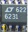
| ☐ | IC | SOIC-8 | LT6231 dual op-amp | 1 | LT6231 ESD!!! |
|
| ☐ | Resistor | 1/6W | 100 1/6W 5% | 2 | br-blk-br-gld |

|
| ☐ | Resistor | 1/4W | 4.99 k 1/4W 1% | 2 | y-w-w-br-br |

|
| ☐ | wire | Cutoff | shunt wire (cut-off lead) | 2 |
Go to Top of Page
Detailed Build Steps
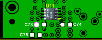
Step_Install Bottomside Caps and IC
| Check | Designation | Component (top/bottom) | Orientation | Marking | Image | Band | Notes |
|---|---|---|---|---|---|---|---|
| ☐ | C73 | 0.1 uF ((bottom)) | (smt) black stripe |
|
any | ||
| ☐ | C74 | 0.1 uF ((bottom)) | (smt) black stripe |
|
any | ||
| ☐ | C75 | 0.1 uF ((bottom)) | (smt) black stripe |
|
any | ||
| ☐ | U11 | LT6231 dual op-amp (top) | (or LT6221) | LT6231 ESD!!! |
|
any | Some kits may substitute 6221 |
Go to Top of Page
Step_Install Topside Resistors and Caps
Note: the two 100 ohm resistors (R57 and R60) in series with the ouputs are there because the op-amps don't like to drive purely capacitive loads - it degrades the phase margins.
Note also that these are the smaller 1/6Watt resistors; not 1/4 watt variety.
| Check | Designation | Component (top/bottom) | Orientation | Marking | Image | Band | Notes |
|---|---|---|---|---|---|---|---|
| ☐ | C43 | 4.7 uF 10% 16V X7R RAD (top) | 475 |
|
any | ||
| ☐ | C44 | 220 pF 5% (top) | 221 |
|
any | ||
| ☐ | C45 | 220 pF 5% (top) | 221 |
|
any | ||
| ☐ | R56 | 4.99 k 1/4W 1% (top) | N-S | y-w-w-br-br |
|
any | |
| ☐ | R57 | 100 1/6W 5% (top) | E-W | br-blk-br-gld |
|
any | |
| ☐ | R59 | 4.99 k 1/4W 1% (top) | N-S | y-w-w-br-br |
|
any | |
| ☐ | R60 | 100 1/6W 5% (top) | E-W | br-blk-br-gld |
|
any |
Go to Top of Page
Step_Install Jack and I/Q Shunts
In both the RX op amp and TX QSE sections, the jumper links on the I/Q input and outputs should ideally be fitted crossed over. That provides compatibility with all versions of PowerSDR. For Rocky and Winrad it is necessary to use the 'swap IQ' functions in their set up. If you jumper them straight across fine for Rocky and Winrad, but you will not be able to use any version of PSDR. (Author wired for Rocky)
Some builders (author included) have encountered issues in this setup and discovered that the only the TX leads should be crossed, leaving the RX leads uncrossed. Be prepared to change these should you encounter this issue.
Also, do not be confused with the terminology here: "Line-In (as silkscreened on the PCB" signifies a connection point for connecting to the Sound card's "Line-in jack". Remember: for the RXTX, "Line-In" goes to "Line-In" and "Line-Out" (see TX OpAmps) goes to "Line-Out"
| Check | Designation | Component (top/bottom) | Orientation | Marking | Image | Band | Notes |
|---|---|---|---|---|---|---|---|
| ☐ | J4 | 3.5mm stereo jack - PCB mount (rt-angle) (top) |
|
any | |||
| ☐ | JP2a | shunt wire (cut-off lead) (top) | any | ||||
| ☐ | JP2b | shunt wire (cut-off lead) (top) | any |
Go to Top of Page
Completed Photos
Progressive Schematic
Where are we in our progress towards the finish line? Click here to view the entire schematic with the completed stages shaded in a yellowish tinge and the remaining stages tinted in blue (the current stage is untinted).
Test the RX Opamps and Output Stage
RX Opamps and Output - Current Draw
Measure the current draw of the board with both USB and regular power applied.
Go to Top of Page
Test Steps (if any)
| Step | Test Point | UOM | Nominal | Author's | Builder's |
|---|---|---|---|---|---|
| 0 | Current drawn | mA | < 25 | 20.7 |
Go to Top of Page
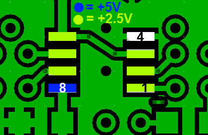
RX Opamps and Output - Pin Voltage Tests
Test pin voltages WRT regular ground, as per graphic
As usual, if you are having any problems with this stage, be sure to measure the pin voltages two ways: first, measure each pin at the pin itself (on the IC). Then take a second measurement at the pin pad (on the board). If those two measurements do NOT agree, you very likely have a soldering issue.
Go to Top of Page
Test Steps (if any)
| Step | Test Point | UOM | Nominal | Author's | Builder's |
|---|---|---|---|---|---|
| 1 | Pin 1 | Vdc | 2,5 | 2.67 | |
| 2 | Pin 2 | Vdc | 2.5 | 2.5 | |
| 3 | Pin 3 | Vdc | 2.5 | 2.5 | |
| 4 | Pin 4 | Vdc | 0 | 0 | |
| 5 | Pin 5 | Vdc | 2.5 | 2.5 | |
| 6 | Pin 6 | Vdc | 2.5 | 2.5 | |
| 7 | Pin 7 | Vdc | 2.5 | 2.65 | |
| 8 | Pin 8 | Vdc | 5 | 4.95 |
Go to Top of Page
RX Opamps and Output - OpAmp Function Test
Test Setup
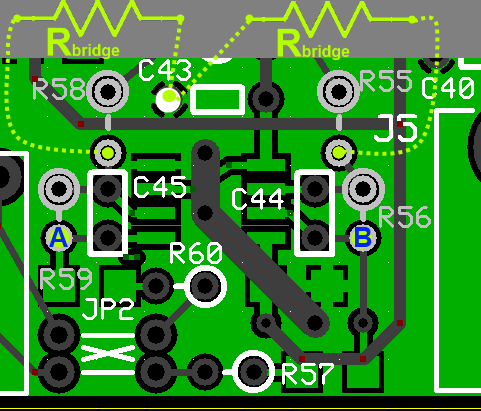
In this test, you will test the DC gain of each of the op-amps by connecting a 10k bridging resistor Rb from each op-amp inverting input to circuit regular ground. Introducing the "bridging" resistor Rb will result in a test current equal to 2.5 / Rt, which will be balanced by the current fed back from each op-amp's output through each feedback resistor, Rf (i.e., R56 or R59). Each op-amp output will increase in voltage by 2.5 * Rf/ Rb from the nominal DC level of 2.5 volts.
(If you have not yet built the TX Op Amp stage, the10k bridging resistor (Rb) will be available for your use)
Test the First OpAmp
- Power up the circuit and measure the voltage at pin 1 of the op-amp (hairpin of R59). It should be ~2.5 Vdc
- Power off and use clip leads to connect Rb between the hairpin of R58 and circuit ground (the left lead of C43 is a convenient ground). This provides an input resistance(Ri) of10 kΩ to the op-amp.
- Power up and measure the output voltage (WRT regular ground) at the hairpin of the feedback resistor R59. You should get: ~3.75 Vdc at R59 hairpin.
- Remove Rb and the output voltage at R59 should go back to ~2.5 Vdc.
Test the Second OpAmp
- Power up the circuit and measure the voltage at pin 7 of the op-amp (hairpin of R56). It should be ~2.5 Vdc
- Power off and use clip leads to connect Rb between the hairpin of R55 and circuit ground (the left lead of C43 is a convenient ground). This provides an input resistance(Ri) of 10 kΩ to the op-amp.
- Power up and measure the output voltage (WRT regular ground) at the hairpin of the feedback resistor R56. You should get: ~3.75 Vdc at R56 hairpin.
- Remove Rb and the output voltage at R56 should go back to ~2.5 Vdc.
The diagram below shows the test points. The yellow dots show the Rb connection points for each "side" of the opamps. The dots marked "A" and "B" show the measurement points for the output voltages for Each "side" of the OpAmps.
An Excel spreadsheet with a calculator for this test is available for you to plug in your bridging resistor ohms (Rt) and your pin 1 or pin 7 normal voltages (Ebias) and predict the expected voltage when bridged (Eout).
Go to Top of Page
You can use the simple calculator below for this test. All you need to do is plug in your bridging resistor ohms (Rt) and your pin 1 or pin 7 normal voltages (Ebias) and predict the expected voltage when bridged (Eout).
Enter the Bridge Resistance (Rb) you Used:
(Feedback Resistance is: 4990)
(Input Resistance is: 10)
Calculated Output Voltage is: (click the compute button to calculate)
Test Steps (if any)
| Step | Test Point | UOM | Nominal | Author's | Builder's |
|---|---|---|---|---|---|
| 1 | Measure "A" (R59) (normal) | Vdc | 2.5 | 2.67 | |
| 2 | Measure "A" (R59) (R58 bridged with 10k to bround) | Vdc | 3.75 | 3.92 | |
| 3 | Measure "B" (R56) | Vdc | 2.5 | 2.65 | |
| 4 | Measure "B" (R56) (R55 bridged with 10k to bround) | Vdc | 3.75 | 3.89 |
Go to Top of Page
RX Opamps and Output - RX Test
Prepare an SDR program for RX (author recommends Rocky for the Windows XP crowd; WinradHD for other Windows OS). This usually involves downloading and installing the program; selecting the desired soundcard for the (STEREO) input of the I and Q signals from the board; and connecting the board to the soundcard with a stereo cable with 1/8" stereo plugs on either end.
The stereo cable should be connected between the PC sound card's "Line-In" input and the Ensemble RXTX's (output) jack (silkscreen-labeled "Line-In" on the board).
Once the SDR program is ready, connect the USB cable from your PC to the board, connect the 12V power to the board, and connect a 50 ohm antenna to J6.
Start the SDR program and adjust the LO frequency to the desired center frequency. You should see signals in the displayed spectrum. If there is a contest going on at test time, you will be even more impressed with the RX.!
Note: for either SDR program to work with the Ensemble RXTX, you MUST have installed the driver (libusb) for the Microcontroller's USB functionality. For WinradHD, you will also need to have downloaded and saved in the same directory as WinradHD, the EXTIO_Si570.dll file.
If you are seeing perfect mirror inages of the signals either side of the center frequency, you should review the information in the Image Rejection Hints page.
Ground Loops and Humps
If you experience a large "hump" at the center frequency or several spurii on the spectrum, you may be the victim of ground loops.
Alan G4ZFQ has an excellent article on the effects of ground loops on the SDR and how to minimize/avoid them. (OK, Alan, so it's "minimise"!)
Go to Top of Page
Test Steps (if any)
Go to Top of Page