Softrock Lite II Home - Softrock Lite II RX
Band: 20m
Introduction
Announcement - Official Site
This site is now the officially maintained site for the Softrock Lite II kit. The previous documentation on www.wb5rvz.com is no longer being maintained. If you are curious, you can still pop over to the previous site to see the original documentation, but be advised that it is no longer being maintained there.
This set of builders notes is replaces and supercedes the notes for the original SR Lite II design, now documenting a combined kit with all of the components required to do any of the five available options (post 1 Jun1 2010). The original design's schematic dates back to December 2009. The current design's schematic is depicted in the Schematic Section, below.
The Softrock Lite II, the sequel to the SR Lite V6.2 series , provides an economical entry-level kit for the ham or SWL who wants to experiment with Software Defined Radio (SDR).
The Lite II circuit board size is 2.5 inches by 0.9 inches. All SMT components are mounted on the bottom of the board .
Ordering Information
Prices and availability of the kit are found at the Softrock Ordering Website.
This kit was originally offered in several versions, corresponding to bands of interest. It has, since, changed over to the Combined Lite II. This "combined" kit will include all components needed to build the kit as a 160m, 80m, 40m, 30m, or 20m receiver. The 15m option is no longer offered. The builder can decide which kit to build at commencement of the build; the parts for any of the options are included in the shipment. The Combined Lite II kit will be priced at $20 plus $1 for US postage or $2 for DX postage.
As of 11 June, 2010, the options in this series will include:
-
40m kit option (the example used herein)
-
- 40m kit will tune the following ranges:
- 40m when used with a soundcard that samples at 48 kHz - 7.032 to 7.08 MHz
- 40m when used with a soundcard that samples at 96 kHz - 7.008 to 7.104 MHz
-
80m kit option
- 80m kit will tune the following range:
- 80m when used with a soundcard that samples at 48 kHz - 3.49825 to 3.54625 MHz
- 80m when used with a soundcard that samples at 96 kHz - 3.47425 to 3.57025 MHz
-
160m kit option
- 160m kit will tune the following range:
- 160m when used with a soundcard that samples at 48 kHz - 1.819 to 1.867 MHz
- 160m when used with a soundcard that samples at 96 kHz - 1.795 to 1.891 MHz
-
30m kit option
- 30m kit will tune the following range:
- 30m when used with a soundcard that samples at 48 kHz - 10.100 to 10.148 MHz
- 30m when used with a soundcard that samples at 96kHz - 10.076 to 10.172 MHz
-
20m kit option
- 20m kit will tune the following range:
- 20m when used with a soundcard that samples at 48 kHz - slightly below 14.024 to 14.070 MHz
- 20m when used with a soundcard that samples at 96 kHz - slightly below 14.00 to 14.094 MHz
The 30m and 20m kits will all make use of 1/3 sub- harmonic sampling.
Prices for these kits are found at the Softrock Ordering site.
Original Versions of SR Lite II
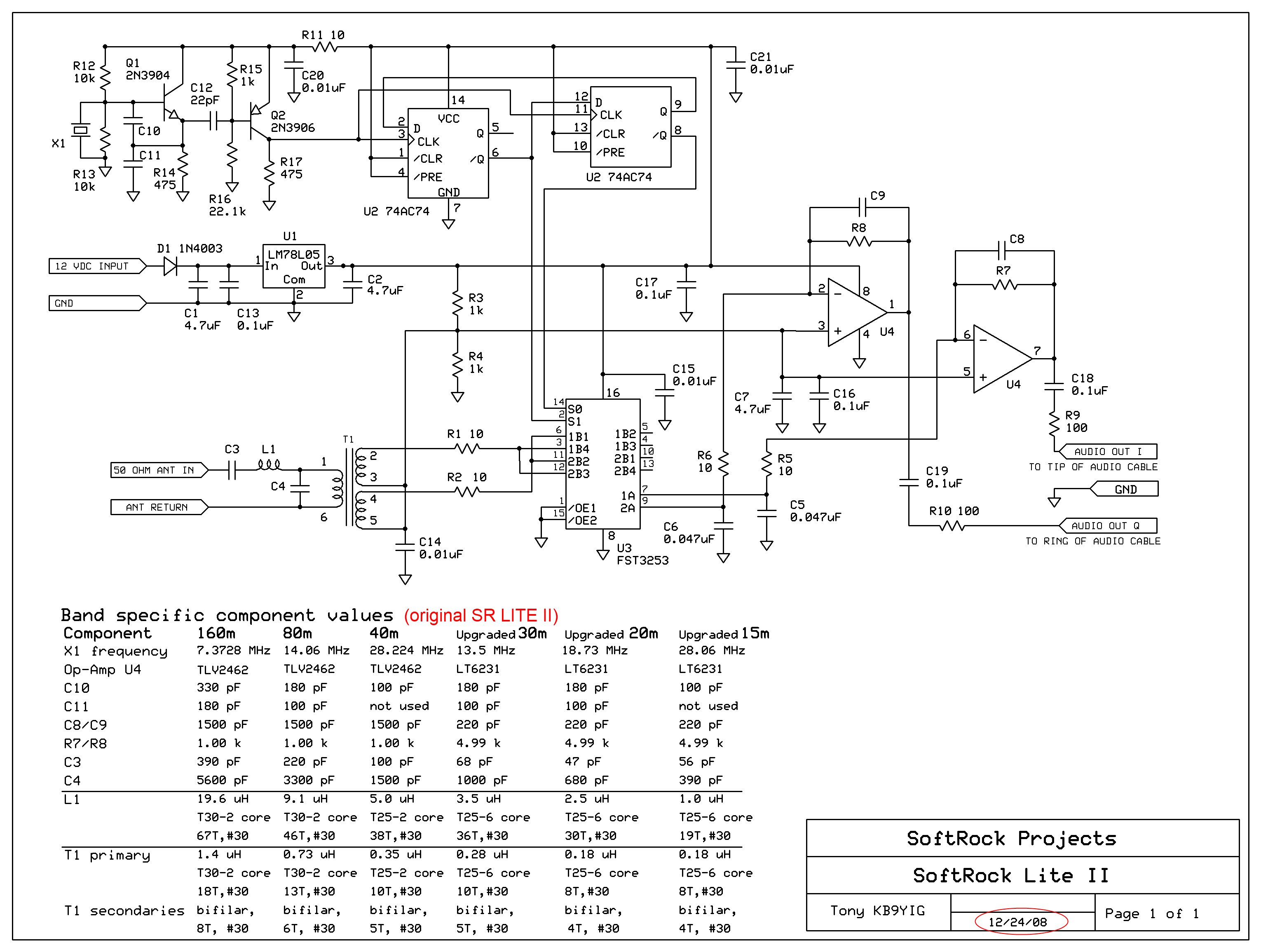
Before the current Combined SRLite II, the SR Lite II came in six versions corresponding to the 160, 80, 40, 30, 20, and 15m bands. These versions were described in the common schematic, which had a table of band-specific component values. The changes from that schematic to the current version are summarized below:
- Drop 15m option
- X1 now 14.089MHz for 80m.
- C8/C9 no longer band-specific; now 390 pF
- R7/R8 no longer band-specific; now 4.99k
- R5 and R6 are now band-specific (49.9Ω on 160, 80, 40; 10Ω on 30, 20)
- Toroids all go to T30-6
- New L1 and T1 winding info for all (all have same uH as original versions, except 30m T1, which goes to 0.18 uH)
- U4 no longer band-specific - it is LT6231 in all options
Original SR Lite II Builders Notes
The original notes were compiled into a PDF file by Philippe F6CZV for those who are still working with the original, now superceded SR Lite (non-combined) kit. Please note that the design of that original kit and the currently offered (from KB9YIG) kit is quite different. Don't get them confused!
Note: SoftRock IF Lite II
Tony also offers several versions of the Softrock Lite II kit that provide panadaptor capability on a number of popular legacy transceivers by tapping into the IF. The versions and the associated IF frequencies are outlined in the table below:
| Rig IF Freq | Xtal Freq | SR Lite Freq |
|---|---|---|
| 455kHz | 1.856 MHz | 464 kHz |
| 4.195 MHz | 19.6875 MHz | 4.921 MHz |
| 8.215 MHz | 32.768 MHz | 8.192 MHz |
| 8.83 MHz | 35.2512 | 8.812 MHz |
| 9.015 MHz | 11.981 MHz |
8.985 MHz (1/3 subharmonic sampling) |
| 10.695 MHz | 14.2764 MHz |
10.707 MHz
(1/3 subharmonic sampling)
|
| 10.707 MHz | 14.299 MHz |
10.724 MHz
(1/3 subharmonic sampling)
|
The schematic for this SR IF Lite II kit is essentially the same as the schematic of the SR Lite II combined kit documented herein and these build notes can be used for the IF version.
(Components required for specific IF options are now included in the printed BOMs in these notes.)
Video of Build for 30m Option
Alan Wolke, W2AEW, has an excellent video showing his build of the 30m option of this kit. Excllently and informatively done, it is worth the watch:
Printable PDF of Build Notes
Click here to download a printable pdf file of the build notes (as of 3/22/2011_
General Info
This kit is for the 20m band and it will tune the following calculated range based upon a crystal frequency of 18.73 MHz:
- When used with a soundcard that samples at 48 kHz (and doesn't have a lowpass filter cutoff below 24 kHz): 14.0235 - 14.0715
- When used with a soundcard that samples at 96 kHz (and doesn't have a lowpass filter cutoff below 48 kHz): 13.9995 - 14.0955
Theory of Operaton
Many thanks to Jan G0BBL and Tony KB9YIG for their input to this and the stages' theoretical discussions.
- This 20m receiver is patterned on the classic "direct conversion" receiver, in that it mixes incoming RF down to audio frequencies by, in effect, beating the RF against a Local oscillator such that the mixer products are in the sub 100 kHz range.
- Unlike the traditional DC receiver, the SDR does not "tune" the local oscillator's frequency to beat up against a desired RF signal. Instead, the local oscillator is at a fixed frequency of 18.73 MHz.
- As a result, the (baseband) mixer products can vary in frequency from zero to +/- some theoretically high super-audio frequency. In fact, the practical limit is one-half the soundcard's maximum sampling rate.
- The "tuning" (and demodulation and AFC and other neat radio things) happen in the software part of the Software Defined Radio. It is the magic of Software that makes for the extraordinarily high selectivity in the direct conversion hardware (which is notorious for great sensitivity but terrible selectivity).
- The software requires the mixer's baseband products to be provided to the PC as two separate signals, each identical to the other, except that they are 90 degrees apart in phase ("in quadrature"). The SR Lite II achieves this by dividing the local oscillator's frequency by 4 (with attendant phase shifts to achieve quadrature).
- The output of the divider chain is two signals, I (In-Phase) and Q (Quadrature), identical in all respects but phase i.e., they are "in quadrature"). For this 20m option, their frequency is 4.6825 MHz
- RF from the antenna is bandpass-filtered for the 20m band.
- The two quadrature signals from the Divider stage are fed into the mixer stage. The 4.6825 MHz quadrature signals from the divider in the 20m option are rich in harmonics. The third harmonic (14.0475) is what is actually used in the mixer stage.
- The mixer stage mixes the bandpass-filtered RF down to two baseband signals that are also in quadrature and otherwise identical to each other.
- The two baseband signals are provided to an amplifier stage where they are amplified and low-pass filtered to levels acceptable to the PC's soundcard stereo line-in inputs.
- A soundcard which can sample 48 kHz, can digitize an incoming "chunk" of baseband signals from 0 to 24 kHz. Such a soundcard, using its stereo line-in inputs for the I and Q signals, will yield an effective bandwidth of 48 kHz: 24 kHz above the center frequency and 24 kHz below the center frequency. The SDR software in the PC manipulates the digitized I and Q signals to deliver, demodulate, condition, and filter signals within this 48 kHz spectrum. Soundcards capable of higher sampling rates (e.g. 96 kHz or 192 kHz) will yield proportionately wider bandwidth, provided their internal audio filters do not cut off the higher audio frequencies.
- Mike Collins KF4BQ (whose photos of the completed board are found further on in this page) has performed extensive tests on this receiver and has found it to be an exceptionally powerful receiver. Considering the cost, nothing out there can beat it!
Schematic
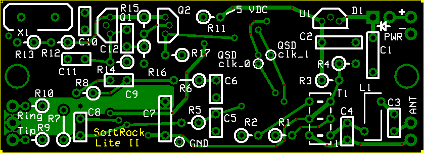
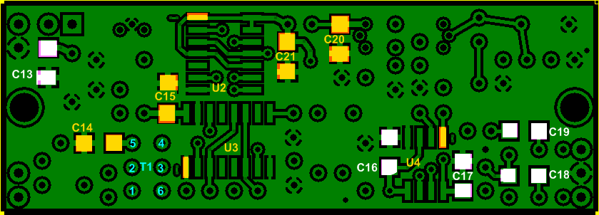
Board Layouts
Topside
Underside
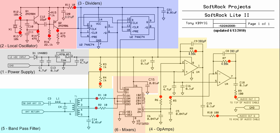
Build Stages
This kit is built in stages, with each stage being testable upon completion.
The stages in the build are, in build order:
- Power Supply
- Local Oscillator
- Divider
- Operational Amplifiers
- Band Pass Filter
- Mixer
- External Connections
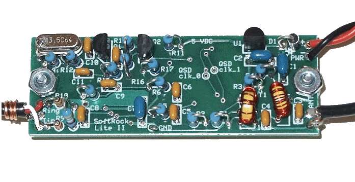
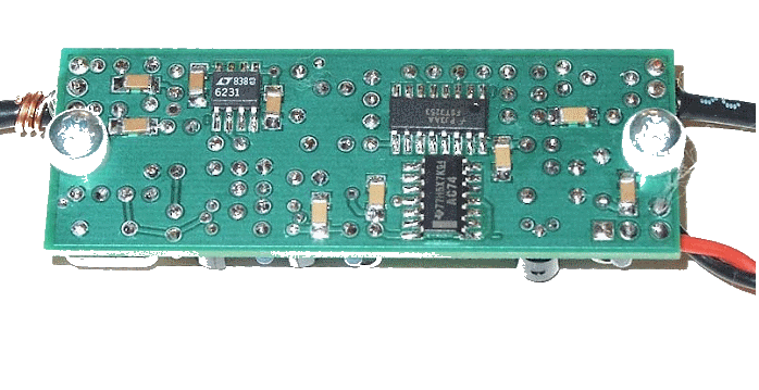
Completed Images
Note: the completed pictures are of the 40m option, which the author built. Other band options (which the author did not build) will appear slightly different (especially the inductors, whose windings and cores will vary by band) for the band-specific components.
Topside
Underside
Background Info
Tools
Winding Inductors
This page has the following inductors:
- L1
COIL: 2.5uH 26T #30 on T30-6 (yellow)
Using approximately 16 inches of #30 wire, wind 26 turns on a 0.30 inch od T30-6 (yellow) ferrite. Inductance = 2.50 uH. - T1
XFRMR: 0.18uH 8T/4T bifilar #30 on T30-6 (yellow)
Primary: Using approximately 7 inches of #30 wire, wind 8 turns on a 0.30 inch od T30-6 (yellow) ferrite.
Secondary: Using a total of 7 inches of #30 wire, wind 4 turns , bifilar, on the ferrite in the same direction as the primary winding. Inductance of the single winding (usually the primary) is 0.18 uH.
To learn how to wind coils and transformers, please read the
- tips from the experts and then
- view the excellent videos on KC0WOXs Website
- or take a read of Dinesh's VU2FD guidelines.
- You can review the common construction techniques for inductors for details on deciphering the winding specifications, core specifications,and construction of toroidal and binocular inductors.
Component Identification
After soldering problems, the most common cause of trouble in kit building is the installation of the incorrect component. Most often this is the case with resistors (hint - if voltage or current draw tests are way out of whack, suspect resistors or solder bridges). Invest in a cheap multimeter and MEASURE the resistance. As Pete, M0FMT, said: " ... then you don't have to worry about this modern trend of poor identification of components. I doubt you will find an issue with Tony's kits but measuring is best. A cheap OVA meter costs 2 or 3 bucks and a simple cap bridge is easy to build. (you can search E-Bay for "L/C/F Inductance Capacitance High Precision Meter" and will find several digital L/C meters for $20-$30) These two bits of kit are worth there wieght in gold. Oh and most meters have diode and transistor testers build in... remarkable when you think back to the darkages when I were a lad."
It cannot be overstressed: do not rely solely on the color codes for identification of the correct resistor; ALWAYS measure with your ohmmeter as a double check. Measure twice, cut once.
Soldering
If you are not experienced at soldering (and even if you are somewhat experienced at soldering), refer to excellent tutorial on basic soldering techniques by Tom Hammond N0SS (SK).
This video provides some excellent hints at soldering (and de-soldering) SMT components:
The video below describes techniques for soldering SOIC 14 (and 16 and 8) SMDs
View the above in full-screen mode on Youtube.
You may also want to review the information from the HamNation series on George, W5JDX, and his build of the Softrock Ensemble RXTX. He uses an inexpensive heat gun and Solder paste to install SMT capacitors and ICs. The Session where he introduces the process is in Episode #70 at 36 minutes, 30 seconds into the podcast.
For the more adventurous, there is a process using solder paste and an electric oven called the reflow process, which can be used to install all the SMT chips to one side of the PC Board. This is documented by Guenael Jouchet in the following Youtube segment:
- Read the Primer on SMT Soldering at the Sparkfun site. It is a very good read and it speaks great truths. Then take the time to watch the video tutorial on soldering an SOIC SMD IC.
- Solder Stations. Don't skimp here. Soldering deficiencies
account for 80 percent of the problems surfaced in troubleshooting. It is preferable
to have an ESD-safe station, with a grounded tip. A couple of good stations that
are relatively inexpensive are:
-
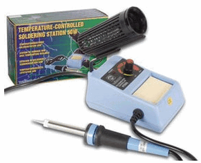 Velleman VTSS5U 50W Solder Station (approx $25 at Frys) (See BGMicro for Spare Tips)
 -
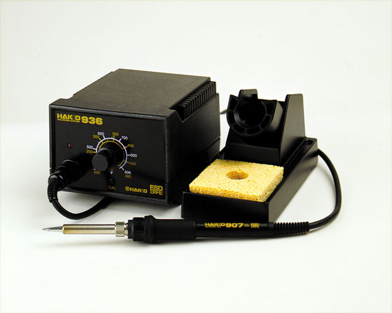 Hakko (Aoyue) 936 ESD Solder Station (under $100)
-
ESD Protection
You may wish to review the message topic beginning at Message 43554 for a common-sense discussion on ESD.
- Avoid carpets in cool, dry areas.
- Leave PC cards and memory modules in their anti-static packaging until ready to be installed.
- Dissipate static electricity before handling any system components (PC cards, memory modules) by touching a grounded metal object, such as the system unit unpainted metal chassis.
- If possible, use antistatic devices, such as wrist straps and antistatic mats (see Radio Shack's Set for $25 or the JameCo AntiStatic mat for $15)).
- Always hold a PC card or memory module by its edges. Avoid touching the contacts and components on the memory module.
- Before removing chips from insulator, put on the wrist strap connected to the ESD mat. All work with CMOS chips should be done with the wrist strap on.
- As an added precaution before first touching a chip, you should touch a finger to a grounded metal surface.
- If using a DMM, its outside should be in contact with the ground of the ESD mat, and both leads shorted to this ground before use.
- See the review of ESD Precautions at this link.
Work Area
- You will need a well-lit work area and a minimum of 3X magnification (the author uses a cheap magnifying fluorescent light with a 3X lens. This is supplemented by a hand-held 10 X loupe - with light - for close-in inspection of solder joints and SMT installation.
- You should use a cookie sheet or baking pan (with four sides raised approximately a half an inch) for your actual work space. It is highly recommended for building on top of in order to catch stray parts, especially the tiny SMT chips which, once they are launched by an errant tweezer squeeze, are nigh on impossible to find if they are not caught on the cookie sheet.
Misc Tools
- It is most important to solidly clamp the PCB in a holder when soldering. A "third-hand" (e.g., Panavise or the Hendricks kits PCB Vise) can hold your board while soldering. In a pinch, you can get by with a simple third-hand, alligator clip vise. Jan G0BBL suggests "A very cheap way is to screw a Large Document Clip to a woodblock which will clamp the side of a PCB."
- Magnifying Head Strap
- Tweezers (bent tip is preferable).
- A toothpick and some beeswax - these can be used to pickup SMT devices and hold them steady while soldering.
- Diagonal side cutters.
- Small, rounded jaw needle-nose pliers.
- Set of jewelers' screwdrivers
- An Exacto knife.
- Fine-grit emery paper.