Ensemble RX II (HF/LF) Home -
Band: HF
Announcement - Official Site
This site is now the officially maintained site for the Ensemble RX II kit. The previous documentation on www.wb5rvz.com is no longer being maintained. If you are curious, you can still pop over to the previous site to see the original documentation, but be advised that it is no longer being maintained there.
Design Change and New PCB Layout
FiveDash have announced a new board and associated changes to schematics and Bils of Material. Please see the Yahoo Softrock40 reflector, message #75035 for details. If your board is dated 6/20/13, you will need to refer to that message to identify changes to these notes. I have updated the affected steps in the affected stages (LO - Install T1 and BPF - Install T2) to show the changes to the board layout.
The other changes have to do with the use of 27 gauge vs #30 gauge wire in certain of the coils L1-L12 in the BPF stage. New winding instructions are now reflected on the relevant BOMs.
de robby wb5rvz
Introduction
General Info
 The Ensemble RX LF/HF kit and its 4.5: X 2" board representing the culmination of a long
line of Softrock SDR receivers from FiveDash, Inc.
(Tony Parks, KB9YIG). The line began with the Softrock 40 RX and went through several iterations of receivers. The most recent receiver was the All-band HF receiver with anautomatically switched bandpass filter. This current kit is a refinement on that kit and further streamlines the kitting process for Tony Parks, the designer and supplier.
The Ensemble RX LF/HF kit and its 4.5: X 2" board representing the culmination of a long
line of Softrock SDR receivers from FiveDash, Inc.
(Tony Parks, KB9YIG). The line began with the Softrock 40 RX and went through several iterations of receivers. The most recent receiver was the All-band HF receiver with anautomatically switched bandpass filter. This current kit is a refinement on that kit and further streamlines the kitting process for Tony Parks, the designer and supplier.
This kit is for the HF band. You cah switch between the HF and LF band options via the "Band" tab in the menu at the top of this (and each) page.
HF Option
The Ensemble RX LF/HF kit provides coverage of HF ham bands from 160-10m, in four different optional "super bands" (each with underlap and overlap within the parameters of the associated bandpass filter):
- Band 0: 160m - Continuous coverage from 1.8 to 4.0 MHz
- Band 1: 80m and 40m - Continuous coverage from 4.0 to 8.0 MHz
- Band 2: 30m, 20m, and 17m - Continuous coverage from 8.0 to 16 MHz
- Band 3: 15m, 12m, and 10m - Continuous coverage from 16 to 30 MHz
The band coverage is via 4 switchable "bands" ("superbands"). Band switching is performed under program control, in conjunction with programmatic control of the receive frequency. This control is provided by an Atmel ATTiny85 micro-controller, acting as a USB device to control the Si570 programmable oscillator and automatically switch to the appropriate band (0-3) as the frequency changes.
As a welcome improvement over other models, this kit provides pcb-right-angle jacks for all external connections: Antenna, USB from the PC, I/Q output to the PC, and Power to the Board. Thus, once built, the kit can be placed in a suitable enclosure and handled thereafter as a "blackbox peripheral" to the PC.
The design of the Ensemble RX is very similar to the receiver design of its sibling Ensemble RXTX. The major difference is the greater band coverage of the Ensemble RX kit (roughly 4 "superbands" on the RX vs. 1 "superband" on the RXTX).
This kit is an excellent value for both the licensed amateur and the SWL who is comfortable with building electronics kits. The skill level and experience requirements are medium-level because of the small size of the components, the requirement to be able to solder SMT parts, and the requirement to wind and install inductors. Thousands of builders have proven this is not an insurmountable set of requirements. If you are new at this, you should try one of Tony's sub $20 monobander RX kits as a "starter/learner" kit.
Several hams have provided interesting/informative galleries of photos as they have followed these build notes:
Recommended Enclosure
Tom KM5KH offers a very nice enclosure for the Ensemble RX line.
Theory of Operaton
Basic Theory
For a very readable (if somewhat dated) presentation of the fundamentals of SDR receivers, see the presentation by Bob, G8VOI..
Block Diagram

This receiver implements a quadrature sampling detector to produce low frequency I and Q signals for input to the stereo line in inputs of a PC sound card. The I and Q signals are the product of the quadrature sampling detector (QSD) stage, in which bandpass filtered "chunks" of RF are mixed with quadrature clock signals to produce the down-converted I and Q signals. These products (the I and Q pairs) are identical to each other in all respects except phase, where they are 90 degrees apart.
The I/Q products of the QSD ("mixer"), when input to the appropriate SDR program through the PC's STEREO line-in soundcard input, result in a spectrum display on the PC which will show signals arrayed around a "center frequency". This "center frequency" is the frequency of the I/Q outputs from the Quadrature Clock Generators. The bandwidth of the signals either side of the center frequency will be approximately equal to the sampling rate of the PC's sound card. Thus, if the local oscillator is tuned to produce 28.4 MHz to the Quadrature Clock Generators, they will output two signals (I and Q clocks) at 7.1MHz (the "center frequency"). If the PC's sound card has a 48 kHz sampling rate, then the SDR program can translate the QSD's I/Q outputs into a chunk of spectrum that is 24 kHz either side of the center frequency of 7.1 MHz: i.e, 7.076 - 7.124 MHz. If the LF Option is built (by eliminating the HF Jumper and installing the second 74AC74 IC to allow for a divide-by-16), the center frequency resulting from a local oscillator frequency of 3.5 MHz (the lowest for the Si570) will be approximately 218 kHz.
As the user tunes the receiver, varying the frequency of the local oscillator, the micro-controller tracks the frequency and switches the appropriate bandpass filter into the RF chain. The SDR program's display will update to show the new center frequency and adjust the scale to reflect the current +/- bandwidth around that center frequency. At all times, the operator can see all signals that are within this movable "window" (whose total width is 48, 96, or 192 kHz, depending upon the sampling rate of the PC's soundcard).
The receiver is controlled via a USB connection from the PC. This USB connection provides a "USB 5V" bus for the local oscillator and micro-controller. A separate 3.3 V voltage regulator on the 5 USB 5 volt bus provides power to the programmable oscillator, the Si570.
The RX has an Atmel ATTiny85 micro-controller unit which, acting as a USB device, and on the "USB 5V" rail, controls the frequency output of the programmable local oscillator (Si570) and provides two switching signals which can be used to select one of four filter banks in the band pass filter
The output of the local oscillator is at a frequency which is 4 times the desired center frequency of the receiver and is consumed in the Quadrature Clock Generators.
The Quadrature Clock Generators divides the local oscillator frequency by 4 (or, for the LF option, by 16) to produce two clock signals - QSE Clk 0 and QSE Clk 1 - which will be used to clock the QSD stage. These I and Q clock signals are identical in all respects but phase (they are in quadrature - 90 degrees phase separation).
Rf at the antenna jack is filtered through the Bandpass Filter Stage, where one of four "chunks" of the HF (or LF) band is selected by the micro-controller, based upon the tuning of the programmable Local Oscillator. The filtered RF is passed as input to the QSD Stage.
The Quadrature Sampling Detector (QSD) Stage acts very similar to a mixer. It incorporates a high-speed switch that is clocked by the two QSD clock signals from the Quadrature Clock Generators and switches the incoming RF into a RC sampling network. The result is two outputs at low frequency and also in quadrature, which are the down-converted, baseband analogs of the incoming RF signals.
The outputs of the QSD stage are then fed into a pair of high gain Operational Amplifiers to produce the I and Q baseband signals which will be input to the PC soundcard's stereo Line In.
Schematic
Below is the full schematic for the complete kit. In addition, subsets of this schematic will be presented in each build stage, focussing only on the functionality of that stage. Stage-level schematics will have labels indicating "connections" to the subschematics of other stages; you can click on those "connections" to quickly navigate to the indicated stage(s). Author's completed board pictures are based upon an even earlier early version of the pcb (differences were minor).
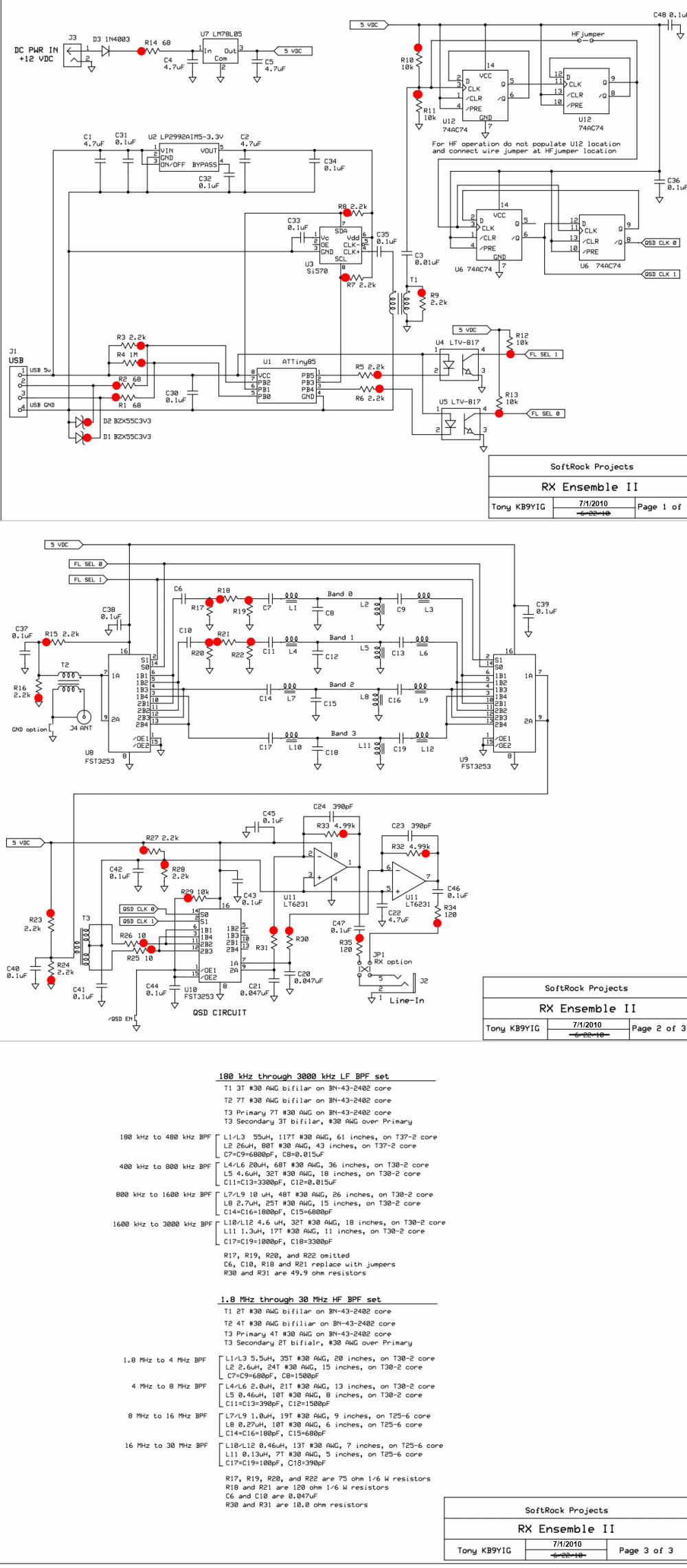
You can also view the original schematics from Tony Parks:
Bill of Materials
The bill of materials for this kit (HF option) is provided in two formats:
- BOM (via the "BOM" tab in the menu at the top of the page): providing summary bill of materials for the components required for this band option (HF option).
- BOM X-Ref(via the "BOM X-Ref" tab above): providing the detailed bill of materials and listing each individual component, along with a cross-reference of the component to the build stage in which it is installed/used.
In addition, there is a complete Inventory ("Inventory" Tab, above) of all of the components, irresective of the kit option, provided in the kit (since the kit provides components for both band options, leaving the decision as to which option to build up to the builder at build time). The builder should first verify all components via the inventory; then use the BOM (for the selected option) to select the parts that wil be used in the actual build of the selected option.
Each build stage will also provide a subset of the overall BOM, listing jost those components required in that stage. Similarly, each step in each build stage will present its own "step-BOM" bill of materials, listing only those components needed in that step.
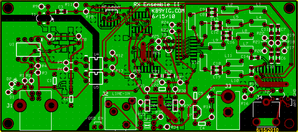
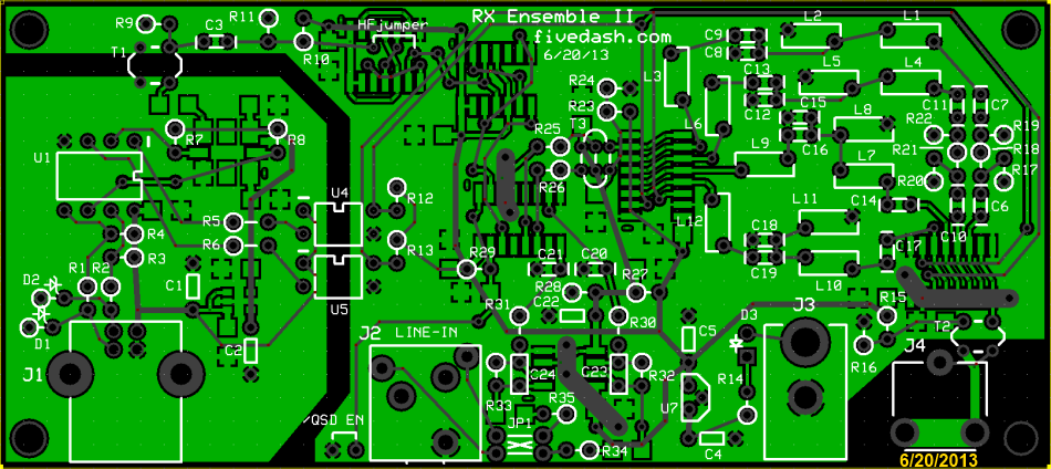
Board Layouts
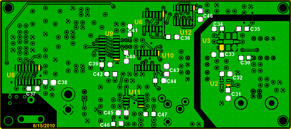
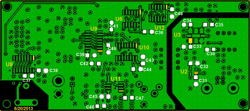
Below are the full board layouts for the kit. Each build stage will present board layout graphics focussed upon the areas of the board (top and bottom) relevant to that build stage. Note that there is a newboard layout, effective 6/20/2013. If your board is dated 6/20/2013, you have the latest board. Both the 6/15/2010 and 6/20/2013 layouts are shown below.
Topside (6/15/2010 version)
Topside (6/20/2013 version)
Underside(6/15/2010 version)
Underside(6/20/2013 version)
Build Stages
This kit is built in stages, with each stage being testable upon completion.
The stages in the build are, in build order:
- Power Supply
- USB Power Supply
- Local Oscillator and Control
- Quadrature Clock Generator
- Auto Band Pass Filters
- Quadrature Sampling Detector
- Operational Amplifiers
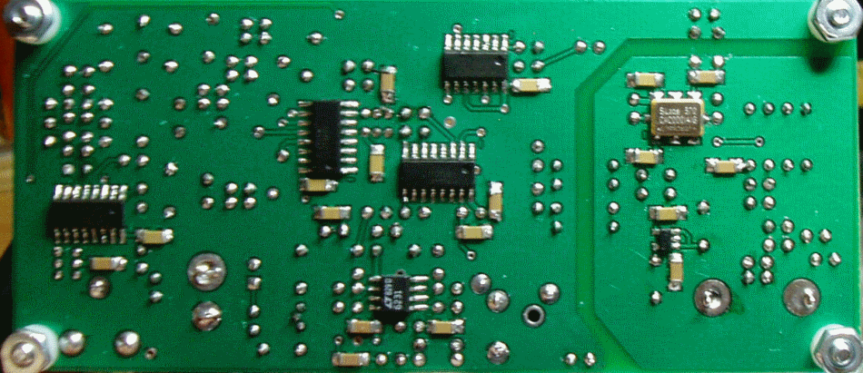
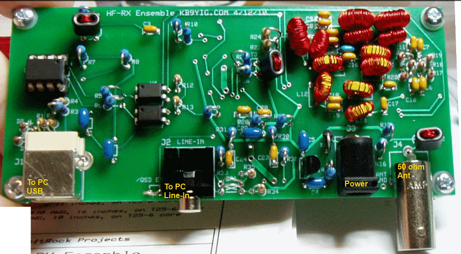
Completed Images
Note: the completed pictures are of the HF option, which the author built. Other band options (which the author did not build) will appear slightly different (especially the inductors, whose windings and cores will vary by band) for the band-specific components.
Topside
Underside