Ensemble RX II (HF/LF) Quadrature Sampling Detector
Band: HF
Introduction
Band Specific Components
This stage involves band-specific components and is currently configured for the HF band. If you need to configure this page for a different band, click on the "Band" tab in the menu above. This would take you to the home page, where you can select the new band and then return to this page.
General Info About the Stage
Theory of Operation
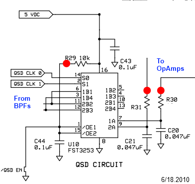
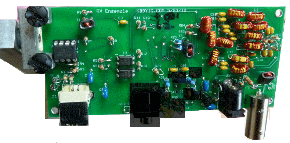
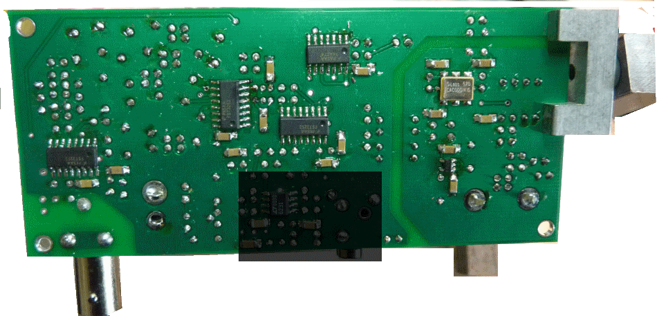
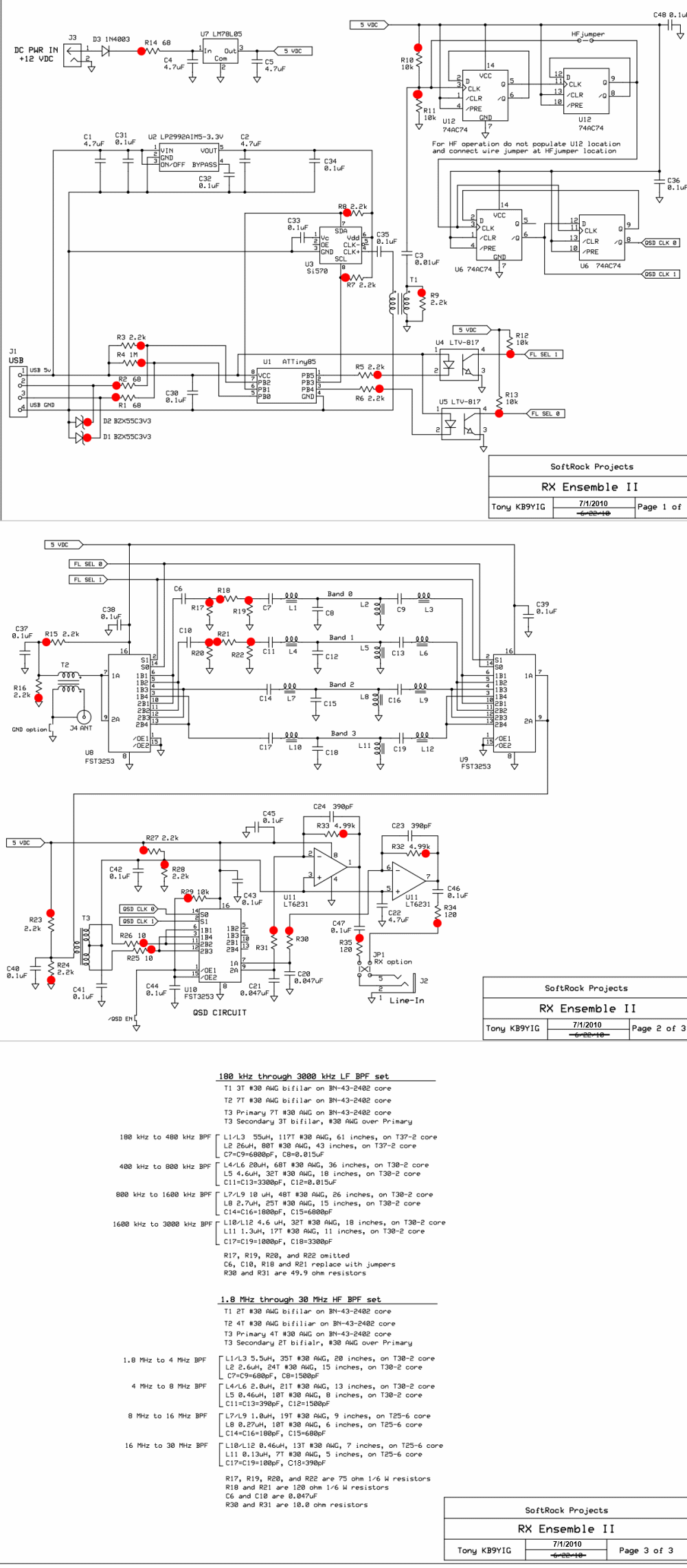
Stage Schematic
Go to Top of Page
Click here for full schematic
(Red dots represent the "hairpin" (or left-hand or topmost) lead of the component)
Summary Build Notes
Quadrature Sampling Detector Bill of Materials
(HF band option)
(details for installation of each component are provided in the step instructions, further down the page)
| Check | Type | Category | Component | Count | Marking | Image |
|---|---|---|---|---|---|---|
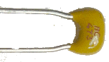
| ☐ | Capacitor | Ceramic | 0.047 uF 5% | 2 | 473 |
|
| ☐ | Capacitor | SMT 1206 | 0.1 uF | 2 | (smt) black stripe |

|
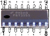
| ☐ | IC | SOIC-16 | FST3253 mux/demux switch | 1 | FST3253 ESD!!! |
|
| ☐ | Resistor | 1/4W | 10 ohm 1/4W 1% | 2 | br-blk-blk-gld-br |

|
| ☐ | Resistor | 1/6W | 10 k 1/6W 5% | 1 | brn-blk-ora-gld |

|
Go to Top of Page
Detailed Build Steps
Install Bottomside Components
| Check | Designation | Component (top/bottom) | Orientation | Marking | Image | Band | Notes |
|---|---|---|---|---|---|---|---|
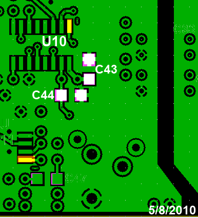
| ☐ | C43 | 0.1 uF ((bottom)) | white pads | (smt) black stripe |
|
any | |
| ☐ | C44 | 0.1 uF ((bottom)) | white pads | (smt) black stripe |
|
any | |
| ☐ | U10 | FST3253 mux/demux switch ((bottom)) | FST3253 ESD!!! |
|
any |
Take extreme care working with this component. Always use ESD precautions.
|
Install Topside Components
Note: the circuit calls for a jumper for the "QSD EN" (QSD Enable) connection. This was installed during the build of the Power Supply to serve as a convenient ground point for testing in subsequent stages. The purpose of the jumper is to enable RX.
Should you have a situation where you would need to disable RX (e.g., while transmitting on a separate TX device), the jumper can be replaced with appropriate switching mechanisms. For RX only, retain the jumper as installed in the Power Supply stage.
| Check | Designation | Component (top/bottom) | Orientation | Marking | Image | Band | Notes |
|---|---|---|---|---|---|---|---|
| ☐ | C20 | 0.047 uF 5% (top) | horiz | 473 |
|
any | |
| ☐ | C21 | 0.047 uF 5% (top) | horiz | 473 |
|
any | |
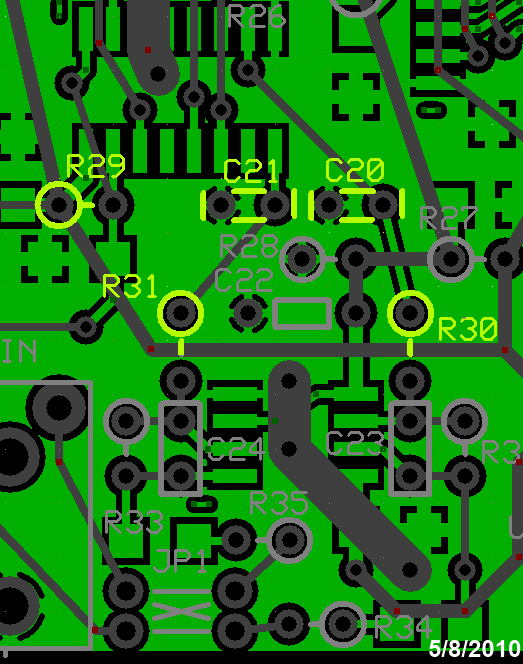
| ☐ | R29 | 10 k 1/6W 5% (top) | W-E | brn-blk-ora-gld |
|
any | was R27 |
| ☐ | R30 | 10 ohm 1/4W 1% (top) | N-S | br-blk-blk-gld-br |
|
HF | |
| ☐ | R31 | 10 ohm 1/4W 1% (top) | N-S | br-blk-blk-gld-br |
|
HF |
Test the Quadrature Sampling Detector Stage
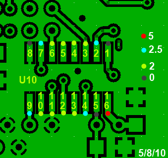
Quadrature Sampling Detector - IC Pin Voltages
Test Notes
It has been observed before that some digital meters are affected by the square wave signals on IC pins and do not always read correctly. The readings you get should approximate 2.5V . The best instrument may be a good oscilloscope. Just be prepared to see slightly different readings on pins 10-13 and 3-6, depending on your DMM (mine is not the best!)
Be sure you have installed the jumper at /QSD EN (back in the Power Supplt stage). This grounds pin 15, enabling the QSD.
Just for a little background information, most of the voltages on U10 pins are derived from the potential divider formed by R27/28 (tested in the Auto Bandpass Filter Stage). If in doubt you can always measure the junction of those two and should get 2.5v as they are equal values across the 5v rail. If one or both were the wrong value, that point would be significantly different. The 2.5v is passed through T3 to the input pins of the multiplexer, and appear on the output pins when the appropriate switch is enabled. Other pins have clock waveforms present, which are relying on the averaging effects of the measuring instrument to give an approximate reading of 2.5v, but this can vary tremendously.
Conduct the Test
Power the board, connect USB to PC
Voltages are measured WRT (regular) ground (/QSD EN shunt )
Bob G8VOI provided thius note concerning these voltages:
Measure pin voltages
It is best to test for these voltages at the actual pins (not the pads), thereby ensuring correct soldering of the pins to the pads.
Go to Top of Page
Test Steps (if any)
| Step | Test Point | UOM | Nominal | Author's | Builder's |
|---|---|---|---|---|---|
| 1 | Pins 1 and 15 (gnd) | V dc | 0 | 0 | |
| 2 | Pins 10, 11, 12, and 13 (40% of 5V rail) | V dc | 2.5 | 2.1 | |
| 3 | Pins 3, 4, 5, and 6 (40% of 5V rail) | V dc | 2.5 | 2.1 | |
| 4 | Pins 7 and 9 (1/2 of 5V rail) | V dc | 2.5 | 2.5 | |
| 5 | Pins 2 and 14 (1/2 of 5V rail) | V dc | 2.5 | 2.5 | |
| 6 | Pin 8 (gnd - /QSD EN, installed in Power Supply Stage) | V dc | 0 | 0 | |
| 7 | Pin 16 (5 V rail) | V dc | 5 | 5 |
Go to Top of Page
Quadrature Sampling Detector - (Optional) QSD Output Test
Power up the board and connect the USB cable
Run CFGSR.exe and dial in a desired center frequency
Inject an RF signal at approximately 10 kHz below the dialed in center frequency
Probe the hairpin leads of R30 and R31 with your dual channel scope
Depending upon your scope's sensitivity, you should see two 10 kHz signals in quadrature.
As you vary the injected signal to move it above the center frequency, you should see the quadrature signals change frequency and, at crossover, switch the leading and lagging positions.
Go to Top of Page
Test Steps (if any)
Go to Top of Page