Ensemble RX II (HF/LF) USB Power Supply
Band: HF
Introduction
General Info About the Stage
This stage installs the power supplies for the USB section of the board. This section is galvanically isolated from the rest of the board, with its own ground plane (the "USB ground"). Voltages measured in this stage are measured with respect to (WRT) this ground and NOT the "regular ground" of the rest of the board. To paraphrase a famous city's motto, "What happens in USB stays in USB!"
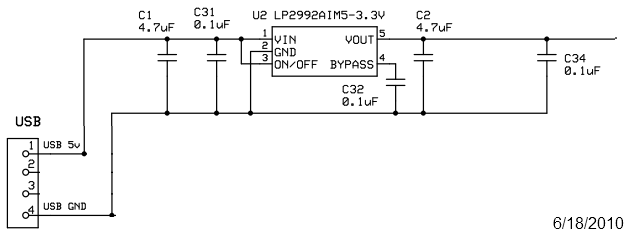
This stage installs the USB connection (with its 5 V bus) and the (very tiny) 3.3V regulator whch translates the USB 5 volts to 3.3V for the Si570 of the next stage..
This stage will present the most difficult SMT soldering challenge to the builder; that voltage regulator is, indeed, tiny! The builder should undertake this stage BEFORE that third cup of coffee and take great pains to avoid launching the little chip off into space (never to be retrieved!)
The 3.3V regulator is, indeed, very tiny. It is found in a rolled up and stapled bottom portion of an antistatic bag. You have to look very closely to find it. You do not want to do, as the author did, toss the chip out with the little rolled up bag!
Theory of Operation
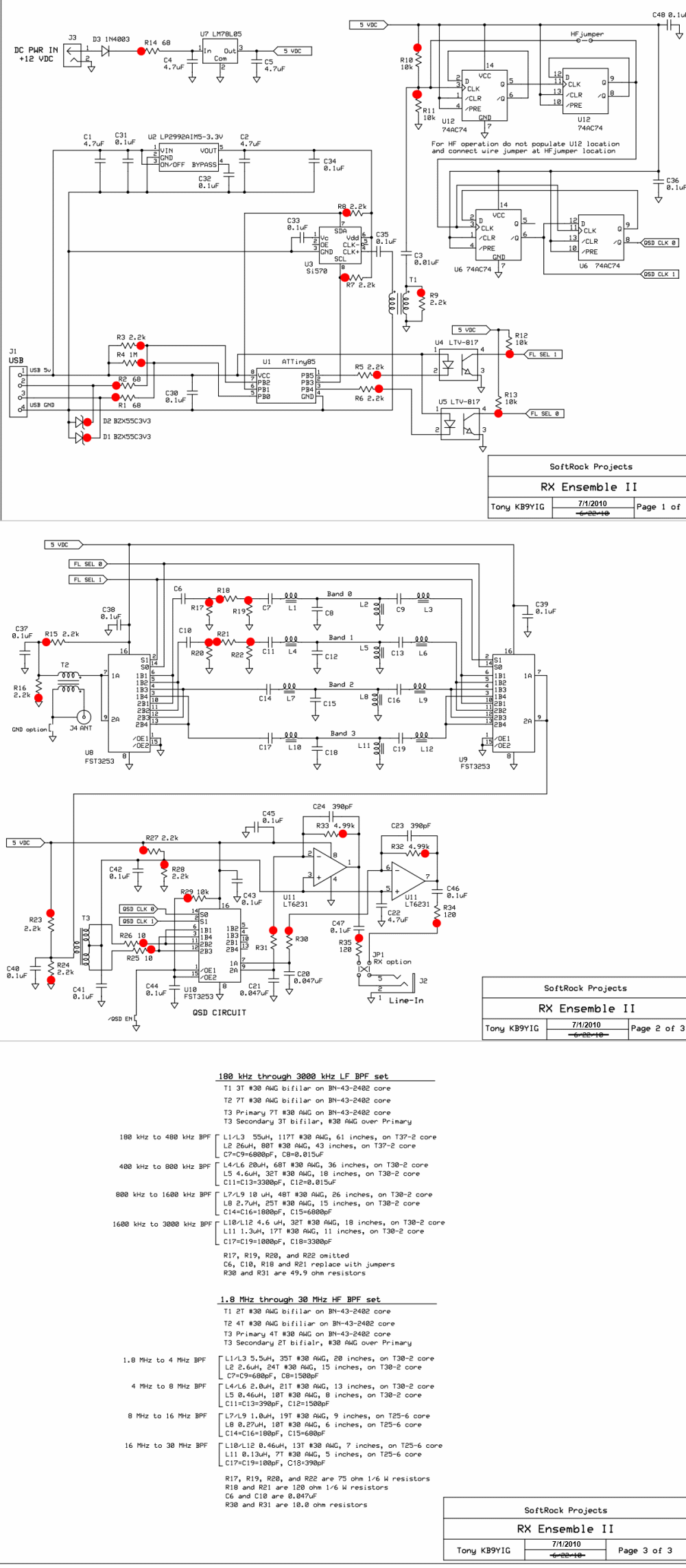
Stage Schematic
Go to Top of Page
Click here for full schematic
(Red dots represent the "hairpin" (or left-hand or topmost) lead of the component)
Summary Build Notes
USB Power Supply Bill of Materials
(HF band option)
(details for installation of each component are provided in the step instructions, further down the page)
| Check | Type | Category | Component | Count | Marking | Image |
|---|---|---|---|---|---|---|
| ☐ | Capacitor | SMT 1206 | 0.1 uF | 3 | (smt) black stripe |

|
| ☐ | Capacitor | Ceramic | 4.7 uF 10% 16V X7R RAD | 2 | 475 |
|
| ☐ | connector | Jack-RA | USB-B pcb jack (rt-angle) | 1 |
|
|
| ☐ | IC | SOT-23-5 | LP2992AIM5-3.3V regulator | 1 | LFEA ESD!!! |

|
Go to Top of Page
Detailed Build Steps
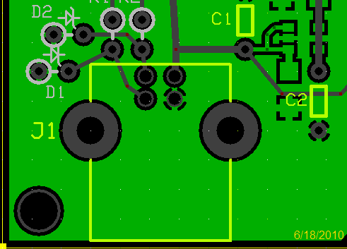
Install Topside Components
You will want to install the topside capacitors (at least) prior to attempting to solder the SMT parts on the underside (there are holes for the ceramic caps which could accidentally be clogged up if you begin with the SMT parts.
The 3.3V regulator is, indeed, very tiny. It is found in a rolled up and stapled bottom portion of an antistatic bag. You have to look very closely to find it. You do not want to do, as the author did, inadvertently toss the chip out with the little rolled up bag!
Due to some problems with recent lots of Si570 devices, Tony has had to pre-mount the Si570s and test them in circuit before sending the kit out. The circuit boards sent out with the Si570 already mounted have a cut in the trace between the 3.3 volt regulator output and the Si570. This is so that the 3.3 volt supply may be verified to be regulating properly before subjecting the Si570 to an over voltage condition. The cut needs to be bridged by scraping the ends of the trace each side of the cut and then soldering in a short wire to bridge the cutl
| Check | Designation | Component (top/bottom) | Orientation | Marking | Image | Band | Notes |
|---|---|---|---|---|---|---|---|
| ☐ | C01 | 4.7 uF 10% 16V X7R RAD (top) | vert | 475 |
|
any | |
| ☐ | C02 | 4.7 uF 10% 16V X7R RAD (top) | vert | 475 |
|
any | |
| ☐ | J01 | USB-B pcb jack (rt-angle) (top) |
|
any |
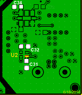
Install Bottomside Components
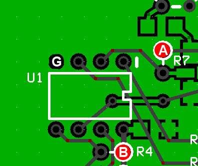
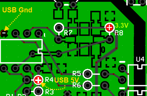
Pay careful attention to the 3.3V regulator. Pins 1 and 3 are at 5V; pin 2 is at ground and nestled snugly between pins 1 and 3.
Per note from fivedash.com
ATTENTION:An SMT capacitor on pin 1 of the Si570 needs to be removed to comply with the NO CONNECT for this pin for the Si570 supplied with the various kits. Having this capacitor mounted on the circuit board degrades the performance of the RXTX transceiver, especially the higher frequency builds of this kit. This capacitor has the following designation for the various kits: C55 for the RXTX Ensemble transceiver, C33 for the RX Ensemble III receiver, C33 for the 6m/4m/2m RX Ensemble receiver, and C33 for the RX Ensemble II receiver.
| Check | Designation | Component (top/bottom) | Orientation | Marking | Image | Band | Notes |
|---|---|---|---|---|---|---|---|
| ☐ | U02 | LP2992AIM5-3.3V regulator ((bottom)) | LFEA ESD!!! |
|
any | ||
| ☐ | C34 | 0.1 uF ((bottom)) | white pads | (smt) black stripe |
|
any | |
| ☐ | C32 | 0.1 uF ((bottom)) | white pads | (smt) black stripe |
|
any | |
| ☐ | C31 | 0.1 uF ((bottom)) | white pads | (smt) black stripe |
|
any |
Test the USB Power Supply Stage
USB Power Supply - Test Resistances
Measure resistances on the power rails to be sure there are no short circuits.
Go to Top of Page
Test Steps (if any)
| Step | Test Point | UOM | Nominal | Author's | Builder's |
|---|---|---|---|---|---|
| 0 | (A) 3.3V rail: R7 barrel to USB Grnd (G) | ohms | >100k | 130k | |
| 2 | (B) USB 5V rail: R4 barrel to USB Ground (G) | ohms | > 1M | 7M and rising |
Go to Top of Page
USB Power Supply - Voltage Test
Connect the USB cable to the PC and to the board.
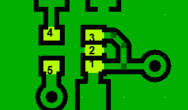
Measure the USB voltages (with respect to the USB ground) at the points indicated on the graphic
Note the two test points are the BARREL ends, not the hairpins, of the resistors (which do not get installed until the next stage).
TroubleShooting the 3.3V Regulator
One case was reported where the regulator tested approximately 1.8 V (as opposed to 3.3V). This was determined to be a faulty bypass capacitor (C32) bypassing pin 4 of the regulator to USB ground).
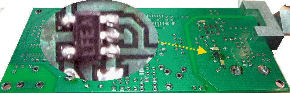
Another case occurred due to a near-invisible solder bridge/"whisker" on the three-pin side of the ID:

Go to Top of Page
Test Steps (if any)
| Step | Test Point | UOM | Nominal | Author's | Builder's |
|---|---|---|---|---|---|
| 0 | 3.3V point R8 (BARREL end - WRT USB Ground) | Vdc | 3.3 | 3.29 | |
| 1 | USB 5V: R4 (BARRELL end - WRT USB Ground) | Vdc | 5 | 5.02 |
Go to Top of Page