Ensemble RXTX - TX Opamps
Band: 30, 20, 17m
Introduction
General Info About the Stage
You may want to follow along with George, W5JDX, as he completes this stage at minute 47:45 of the HamNation podcast #79.
This stage has a pretty large part count.. It consists of four unitary gain op-amps, arranged in pairs, one per stereo line out signal into the board. The left channel's input resolves to two signals: 0° and 180°. The right channel's input resolves to two signals: 90° and 270°.
These four outputs will be muxed together in the Mixer Stage to produce the desired exciter output (thus, the term Quadrature Sampling Exciter (QSE)).
Theory of Operation
(see the Theory of Operation in the TX Mixer (QSE) Stage)
Summary Build Notes
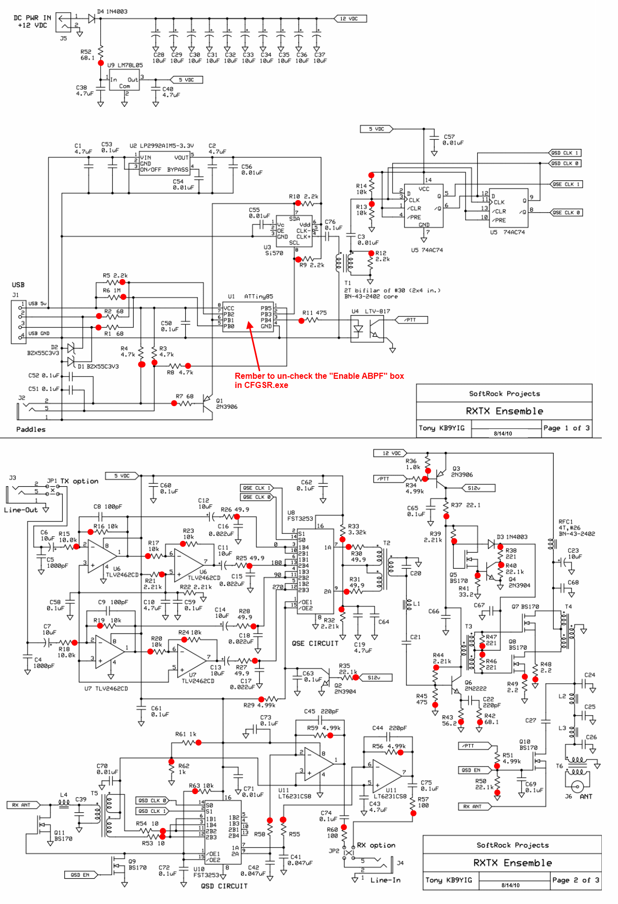
Stage Schematic

Go to Top of Page
Click here for full schematic
(Red dots represent the "hairpin" (or left-hand or topmost) lead of the component)
Board Layouts
Board Top

Go to Top of Page
Board Bottom

Go to Top of Page
TX Opamps Bill of Materials
(30, 20, 17m band option)
(details for installation of each component are provided in the step instructions, further down the page)
Note: The BOM calls for a 100k Ohm resistor that is NOT provided with the kit. That resistor is needed only if the builder wants to perform the OpAmps Functional Test at the end of this stage. If such is the case, the builder must provide their own 100k Ohm resistor.
| Check | Type | Category | Component | Count | Marking | Image |
|---|---|---|---|---|---|---|
| ☐ | Capacitor | Ceramic | 100 pF 5% | 2 | 101 |

|
| ☐ | Capacitor | Ceramic | 1000 pF 5% | 2 | 102 |

|
| ☐ | Capacitor | Ceramic | 0.022 uF 5% | 4 | 223 |

|
| ☐ | Capacitor | SMT 1206 | 0.1 uF | 4 | (smt) black stripe |

|
| ☐ | Capacitor | Ceramic | 4.7 uF 10% 16V X7R RAD | 1 | 475 |
|
| ☐ | Capacitor | Electrolytic | 10uF/16 VDC | 6 |

|
|
| ☐ | Connector | Jack-RA | 3.5mm stereo jack - PCB mount (rt-angle) | 1 |

|
|
| ☐ | IC | SOIC-8 | TLV2462CD dual opamp | 2 | TVL2462CD ESD!!! |

|
| ☐ | Resistor | 1/4W | 49.9 ohm 1% | 4 | yel-wht-wht-gld-brn |

|
| ☐ | Resistor | 1/4W | 2.21 k 1/4W 1% | 2 | r-r-br-br-br |

|
| ☐ | Resistor | 1/4W | 10 k 1/4W 1% | 8 | br-blk-blk-r-br |

|
| ☐ | resistor | 1/6W | 100k 1/6W 5% | 1 | brn_blk_yel_gld |

|
| ☐ | wire | Cutoff | shunt wire (cut-off lead) | 2 |
Go to Top of Page
Detailed Build Steps
Step_Install Bottomside Components
| Check | Designation | Component (top/bottom) | Orientation | Marking | Image | Band | Notes |
|---|---|---|---|---|---|---|---|
| ☐ | U06 | TLV2462CD dual opamp ((bottom)) | TVL2462CD ESD!!! |
|
any | ||
| ☐ | U07 | TLV2462CD dual opamp ((bottom)) | TVL2462CD ESD!!! |
|
any | ||
| ☐ | C58 | 0.1 uF ((bottom)) | (smt) black stripe |
|
any | ||
| ☐ | C59 | 0.1 uF ((bottom)) | (smt) black stripe |
|
any | ||
| ☐ | C60 | 0.1 uF ((bottom)) | (smt) black stripe |
|
any | ||
| ☐ | C61 | 0.1 uF ((bottom)) | (smt) black stripe |
|
any |
Go to Top of Page
Step_Install Topside Components
After installing R21 and R22, you might want to run a quick powered test at the junction (R21 hairpin lead). R21/22 form a voltage divider on the 5 volt rail and you should see one-half the 5 volt rail voltage WRT regular ground (about 2.5 Vdc).
| Check | Designation | Component (top/bottom) | Orientation | Marking | Image | Band | Notes |
|---|---|---|---|---|---|---|---|
| ☐ | R21 | 2.21 k 1/4W 1% (top) | N-S | r-r-br-br-br |
|
any | |
| ☐ | R22 | 2.21 k 1/4W 1% (top) | S-N | r-r-br-br-br |
|
any | |
| ☐ | R15 | 10 k 1/4W 1% (top) | S-N | br-blk-blk-r-br |
|
any | |
| ☐ | R16 | 10 k 1/4W 1% (top) | N-S | br-blk-blk-r-br |
|
any | |
| ☐ | R17 | 10 k 1/4W 1% (top) | W-E | br-blk-blk-r-br |
|
any | |
| ☐ | R18 | 10 k 1/4W 1% (top) | S-N | br-blk-blk-r-br |
|
any | |
| ☐ | R19 | 10 k 1/4W 1% (top) | N-S | br-blk-blk-r-br |
|
any | |
| ☐ | R20 | 10 k 1/4W 1% (top) | W-E | br-blk-blk-r-br |
|
any | |
| ☐ | R23 | 10 k 1/4W 1% (top) | E-W | br-blk-blk-r-br |
|
any | |
| ☐ | R24 | 10 k 1/4W 1% (top) | E-W | br-blk-blk-r-br |
|
any | |
| ☐ | R25 | 49.9 ohm 1% (top) | S-N | yel-wht-wht-gld-brn |
|
any | |
| ☐ | R26 | 49.9 ohm 1% (top) | S-N | yel-wht-wht-gld-brn |
|
any | |
| ☐ | R27 | 49.9 ohm 1% (top) | S-N | yel-wht-wht-gld-brn |
|
any | |
| ☐ | R28 | 49.9 ohm 1% (top) | S-N | yel-wht-wht-gld-brn |
|
any | |
| ☐ | C04 | 1000 pF 5% (top) | 102 |
|
any | ||
| ☐ | C05 | 1000 pF 5% (top) | 102 |
|
any | ||
| ☐ | C08 | 100 pF 5% (top) | 101 |
|
any | ||
| ☐ | C09 | 100 pF 5% (top) | 101 |
|
any | ||
| ☐ | C10 | 4.7 uF 10% 16V X7R RAD (top) | 475 |
|
any | ||
| ☐ | C15 | 0.022 uF 5% (top) | 223 |
|
any | ||
| ☐ | C16 | 0.022 uF 5% (top) | 223 |
|
any | ||
| ☐ | C17 | 0.022 uF 5% (top) | 223 |
|
any | ||
| ☐ | C18 | 0.022 uF 5% (top) | 223 |
|
any | ||
| ☐ | C06 | 10uF/16 VDC (top) |
|
any | |||
| ☐ | C07 | 10uF/16 VDC (top) |
|
any | |||
| ☐ | C11 | 10uF/16 VDC (top) |
|
any | |||
| ☐ | C12 | 10uF/16 VDC (top) |
|
any | |||
| ☐ | C13 | 10uF/16 VDC (top) |
|
any | |||
| ☐ | C14 | 10uF/16 VDC (top) |
|
any | |||
| ☐ | R-TEST | 100k 1/6W 5% (top) | (Not supplied with kit) | brn_blk_yel_gld |
|
any | Not supplied with kit. Only needed for TX OpAmps functional test |
Go to Top of Page
Step_Install IQ-In Jack and Jumpers
In both the RX op amp and TX QSE sections, the jumper links on the I/Q input and outputs should ideally be fitted crossed over. That provides compatibility with all versions of PowerSDR. For Rocky and Winrad it is necessary to use the 'swap IQ' functions in their set up. If you jumper them straight across fine for Rocky and Winrad, but you will not be able to use any version of PSDR. (Author wired for Rocky)
Recently, there have been extensive discussions on the reflector concerning the fact that some builders have a combination of soundcard, software, PC, and operating system in which the jumpers/leads for the TX I and Q signals must be the reverse of the jumpers/leads for the RX I and Q. This has been pretty much a case-by-case experience. We are building a spreadsheet depicting various combinations of the relevant variables (soundcard, program, kit, PS, OS, etc.) and the wiring that "works" for the RX and TX I and Q signals.
| Check | Designation | Component (top/bottom) | Orientation | Marking | Image | Band | Notes |
|---|---|---|---|---|---|---|---|
| ☐ | JP1A | shunt wire (cut-off lead) (top) | any | ||||
| ☐ | JP1B | shunt wire (cut-off lead) (top) | any | ||||
| ☐ | J3 | 3.5mm stereo jack - PCB mount (rt-angle) (top) |
|
any |
Go to Top of Page
Completed Photos
View of Completed Topside

View of Completed Underside

Go to Top of Page
Progressive Schematic
Where are we in our progress towards the finish line? Click here to view the entire schematic with the completed stages shaded in a yellowish tinge and the remaining stages tinted in blue (the current stage is untinted).
Test the TX Opamps Stage
TX Opamps - Current Draw
Measure the current drawn by the 12V power supply with the 12V power connected. (if you have both the 12 V and trhe USB connected, the current drawr will be a little less than it would be without the USB connected.
Go to Top of Page
Test Steps (if any)
| Step | Test Point | UOM | Nominal | Author's | Builder's |
|---|---|---|---|---|---|
| 0 | Current draw | mA | < 35 | 26.6 |
Go to Top of Page
TX Opamps - Pin Voltages
Power up the board and then measure the voltages at each of the pins of the two OpAmp Ics.
You should see the 5V rail voltage at pins 8, 0 Vdc at pins 4, and one half the 5 Volt rail at all other pins. The one-half of the 5v rail is from the voltage divider at R21/R22.
If you do not get these voltages, carefully take and compare the measurements on both the pin itself AND the pin PAD. If you get a different voltage on the pin vs. the pad, re-check your soldering. Check out the resistor values at R21/R22 to be sure they are both the correct value (2.21k) and/or use the utility Voltage Divider Calculator to enter your actual reading and determine what value may have been substituted for the correct value resistor.

Go to Top of Page
Test Steps (if any)
| Step | Test Point | UOM | Nominal | Author's | Builder's |
|---|---|---|---|---|---|
| 1 | Left IC, Pin 1 | Vdc | 2.5 | 2.48 | |
| 2 | Left IC, Pin 2 | Vdc | 2.5 | 2.48 | |
| 3 | Left IC, Pin 3 | Vdc | 2.5 | 2.48 | |
| 4 | Left IC, Pin 4 | Vdc | 0 | 0 | |
| 5 | Left IC, Pin 5 | Vdc | 2.5 | 2.48 | |
| 6 | Left IC, Pin 6 | Vdc | 2.5 | 2.48 | |
| 7 | Left IC, Pin 7 | Vdc | 2.5 | 2.48 | |
| 8 | Left IC, Pin 8 | Vdc | 5 | 4.96 | |
| 9 | Right IC, Pin 1 | Vdc | 2.5 | 2.48 | |
| 10 | Right IC, Pin 2 | Vdc | 2.5 | 2.48 | |
| 11 | Right IC, Pin 3 | Vdc | 2.5 | 2.48 | |
| 12 | Right IC, Pin 4 | Vdc | 0 | 0 | |
| 13 | Right IC, Pin 5 | Vdc | 2.5 | 2.48 | |
| 14 | Right IC, Pin 6 | Vdc | 2.5 | 2.48 | |
| 15 | Right IC, Pin 7 | Vdc | 2.5 | 2.48 | |
| 16 | Right IC, Pin 8 | Vdc | 5 | 4.96 |
Go to Top of Page
TX Opamps - OpAmps Functional Test
This test is similar to the test performed on the RX OpAmps.
You will need a 100k ohm resistor (not supplied with the kit) to perform the test. It involves connecting the 100k ohm resistor between pin 2 and ground for each Tx Opamp chip and measuring the output voltages at pins 1 and 7.
- First, you measure the normal output voltages at pins 1 and 7
- Then you connect the 100k ohm resistor between pin 2 (R15 hairpin) and ground
- Then you remeasure the voltages at pins 1 and 7
- And repeat the process for the second OpAmp, with its pin 2 (R18 hairpin) unbridged and bridged to ground

Go to Top of Page
Test Steps (if any)
| Step | Test Point | UOM | Nominal | Author's | Builder's |
|---|---|---|---|---|---|
| 0 | U6-pin1 (R17 hairpin) - not bridged | V dc | 2.5 | 2.48 | |
| 1 | U6-pin7 - not bridged | V dc | 2.5 | 2.48 | |
| 3 | U6-pin1 (R17 hairpin) - R15 hairpin bridged 100k to ground | V dc | 2.75 | 2.72 | |
| 4 | U6-pin7 - R15 hairpin bridged 100k to ground | V dc | 2.25 | 2.23 | |
| 5 | U7-pin1 (R20 hairpin) - not bridged | V dc | 2.5 | 2.48 | |
| 6 | U7-pin7 not bridged | V dc | 2.5 | 2.48 | |
| 7 | U7-pin1 (R20 hairpin) - R18 hairpin bridged 100k to ground | V dc | 2.75 | 2.72 | |
| 8 | U7-pin7 - R18 hairpin bridged 100k to ground | V dc | 2.25 | 2.23 |
Go to Top of Page
TX Opamps - OpAmp Outputs
If you have (access to) a dual channel scope, you may want to download Michael Keller, DL6iAK's IQ Gen and generate a dual tone quadrature signal for feeding into the "Line Out" Jack.
You can then probe the output resistors (R25-R28) to see the two anti-phase signals produced by this stage.
Go to Top of Page
Test Steps (if any)
Go to Top of Page